HDSP-5538 Avago Technologies US Inc., HDSP-5538 Datasheet - Page 8
HDSP-5538
Manufacturer Part Number
HDSP-5538
Description
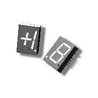
DISPLAY 7SEGMENT HER CC 0.56"
Manufacturer
Avago Technologies US Inc.
Type
Moduler
Specifications of HDSP-5538
Display Type
7-Segment
Common Pin
Common Cathode
Number Of Digits/alpha
+/-1 (overflow)
Size / Dimension
0.67" L x 0.49" W x 0.31" H (17.02mm x 12.57mm x 8.00mm)
Digit/alpha Size
0.56" (14.22mm)
Color
Red
Voltage - Forward (vf) Typ
2.6V
Current - Test
20mA
Millicandela Rating
4.8mcd
Wavelength - Peak
635nm
Power Dissipation (max)
105mW
Package / Case
10-DIP (0.600", 15.24mm), 9 Leads
Number Of Digits
1
Character Size
14.1 mm
Illumination Color
High Efficiency Red
Wavelength
635 nm
Operating Voltage
2.6 V
Operating Current
40 mA
Maximum Operating Temperature
+ 85 C
Minimum Operating Temperature
- 40 C
Luminous Intensity
4800 ucd
Package Type
DIP
Product Length (mm)
17.1mm
Product Height (mm)
8mm
Product Depth (mm)
12.4mm
Character Displayed
Numeric
Emitting Color
Hi-Eff. Red
Forward Voltage
3.5V
Forward Current
40mA
Dominant Wave Length
636nm
Power Dissipation
105mW
Total Thickness
8mm
Reverse Voltage
5V
Mounting
Through Hole
Operating Temperature Classification
Industrial
Pin Count
10
Configuration
Common Cathode
Number Of Elements
5
Peak Wavelength
635nm
Reverse Current
100uA
Lead Free Status / RoHS Status
Lead free / RoHS Compliant
Lead Free Status / RoHS Status
Lead free / RoHS Compliant, Lead free / RoHS Compliant


Electrical
These display devices are composed of eight light emitting
diodes, with light from each LED optically stretched to
form individual segments and a decimal point.
The devices utilize LED chips which are made from GaAsP
on a transparent GaP substrate.
These display devices are designed for strobed operation.
The typical forward voltage values, scaled from Figure 4,
should be used for calculating the current limiting resistor
value and typical power dissipation. Expected maximum
V
maximum power dissipation, may be calculated using the
following V
V
For: I
V
For: 10 mA ≤ I
Temperature derated strobed operating conditions are
obtained from Figures 1 and 2. Figure 1 relates pulse
duration (t
current to maxi mum dc current (I
2 presents the maximum allowed dc current vs. ambient
temperature. Figure 1 is based on the principle that the peak
junc tion temperature for pulsed operation at a specified
peak current, pulse duration and refresh rate should be
the same as the junction temperature at maximum DC
operation. Refresh rates of 1 kHz or faster minimize the
pulsed junction heating effect of the device resulting in the
maximum possible time average luminous intensity.
The time average luminous inten sity can be calculated
knowing the average forward current and relative ef-
ficiency characteristic, K
luminous intensity for a device case temperature of 25°C,
I
I
Example: For HDSP-4030 series
K
For DF = 1/5:
I
8
V
V
V
F
F
F
PEAK
(25°C), is calculated as follows:
(25°C) = [
(25°C) = [
MAX = 1.9 V + I
MAX = 2.15 V + I
values, for the purpose of driver circuit design and
F
= 1.00 at I
≥ 30 mA
= 4.5 mcd/segment
p
F
), refresh rate (f), and the ratio of maxi mum peak
20 mA
20 mA
20 mA
MAX models:
I
AVG
F
≤ 30 mA
PEAK
DC
] [K
] [1.00] [4.5 mcd]
PEAK
(21.8 :)
= 100 mA.
PEAK
(13.5 :)
PEAK
] [I
V DATA SHEET
, of Figure 3. Time average
PEAK
MAX/I
]
DC
MAX). Figure
The time average luminous inten sity may be adjusted for
operat ing junction temperature by the following expo-
nential equation:
I
where T
Mechanical
These devices are constructed utilizing a lead frame in a
standard DIP package. The LED dice are attached directly
to the lead frame. Therefore, the cathode leads are the
direct thermal and mechanical stress paths to the LED
dice. The absolute maximum allowed junction tempera-
ture, T
been established so that the worst case V
exceed this limit.
Worst case thermal resistance pin-to-ambient is 400°C/W/
Seg when these devices are soldered into minimum
trace width PC boards. When installed in a PC board that
provides RT
may be operated at higher average currents as shown in
Figure 2.
Optical
The radiation pattern for these devices is approximately
Lam bertian. The luminous sterance may be calculated
using one of the two following formulas.
L
L
V
Device
-3900
-4030/-4130/-5730/-4200
Device
-4030
-4130
-5730
-3900/-4200
V
V
(T
(cd/m
(footlamberts) =
J
) = I
J
MAX, is 105°C. The maximum power ratings have
J
2
V
= T
)
(25°C) e
A
PIN-A
+ P
D
=
[k(T
less than 400°C/W/Seg these displays
SI
A (m
I
A (ft
v
J
v
+ 25°C)]
(cd)
J-A
(cd)
2
2
)
)
Area/Seg.
mm
2.5
4.4
8.8
14.9
2
K
-0.0131/°C
-0.0112/°C
F
device does not
Area/Seg.
in
0.0039
0.0068
0.0137
0.0231
2
Related parts for HDSP-5538
Image
Part Number
Description
Manufacturer
Datasheet
Request
R

Part Number:
Description:
LED 7-SEG 7.6MM CC HE RED RHD
Manufacturer:
Avago Technologies US Inc.
Datasheet:

Part Number:
Description:
LED 7-SEG 7.6MM CA HE RED RHD
Manufacturer:
Avago Technologies US Inc.
Datasheet:

Part Number:
Description:
LED 7-SEG 7.6MM CA GREEN RHD
Manufacturer:
Avago Technologies US Inc.
Datasheet:

Part Number:
Description:
LED 7-SEG 7.6MM CC GREEN RHD
Manufacturer:
Avago Technologies US Inc.
Datasheet:

Part Number:
Description:
LED DISPLAY HEX 4X7 7.4MM HE RED
Manufacturer:
Avago Technologies US Inc.
Datasheet:

Part Number:
Description:
LED 7-SEG 14.2MM CC HE RED RHD
Manufacturer:
Avago Technologies US Inc.
Datasheet:

Part Number:
Description:
LED BAR GRAPH 10SEG GREEN
Manufacturer:
Avago Technologies US Inc.
Datasheet:

Part Number:
Description:
LED BAR GRAPH 10SEG YELLOW
Manufacturer:
Avago Technologies US Inc.
Datasheet:

Part Number:
Description:
LED DISPLAY 5X7 8CHAR 5MM HE RED
Manufacturer:
Avago Technologies US Inc.
Datasheet:

Part Number:
Description:
LED 7-SEG 14.2MM 2DIG CC HER RHD
Manufacturer:
Avago Technologies US Inc.
Datasheet:

Part Number:
Description:
LED DISPLAY 5X7 8CHAR 5MM GREEN
Manufacturer:
Avago Technologies US Inc.
Datasheet:
Part Number:
Description:
LED DISPLAY 5X7 8CHAR 5MM GREEN
Manufacturer:
Avago Technologies US Inc.
Datasheet:
Part Number:
Description:
LED DISPLAY 5X7 8CHAR 5MM YLW
Manufacturer:
Avago Technologies US Inc.
Datasheet:
Part Number:
Description:
LED DISPLAY 5X7 8CHAR 5MM RED
Manufacturer:
Avago Technologies US Inc.
Datasheet:

Part Number:
Description:
LED DISPLAY 5X7 8CHAR 7MM HE RED
Manufacturer:
Avago Technologies US Inc.
Datasheet: