HDSP-2502 Avago Technologies US Inc., HDSP-2502 Datasheet
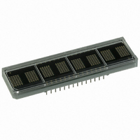
HDSP-2502
Specifications of HDSP-2502
Available stocks


Related parts for HDSP-2502


HDSP-2502 Summary of contents
Page 1
... Multi-level dimming and blanking x TTL compatible CMOS IC x Wave solderable Applications x Computer peripherals x Industrial instrumentation x Medical equipment x Portable data entry devices x Cellular phones x Telecommunications equipment x Test equipment High Efficiency Red Orange HDSP-2112 HDSP-2110 HDSP-2502 HDSP-2500 Yellow Green HDSP-2111 HDSP-2113 HDSP-2501 HDSP-2503 ...
Page 2
... PIN DESIGNATION PIN 1 IDENTIFIER 2.69 (0.106) PART NUMBER DATE CODE [4] HDSP-21XX YYWW 4.79 SYM. (0.189) DIA. 0.51 ± 0.13 (0.020 ± 0.005) NOTES: 1. DIMENSIONS ARE IN mm (INCHES). 2. UNLESS OTHERWISE SPECIFIED, TOLERANCE ON ALL DIMENSIONS IS ± 0.25 mm (0.010 INCH). 3. FOR YELLOW AND GREEN DEVICES ONLY. ...
Page 3
... PIN DESIGNATION PIN 1 IDENTIFIER PART NUMBER DATE CODE [4] HDSP-250X YYWW 19.01 SYM. (0.749) 2.54 ± 0.13 (0.100 ± 0.005) NOTES: 1. DIMENSIONS ARE IN mm (INCHES). 2. UNLESS OTHERWISE SPECIFIED, TOLERANCE ON ALL DIMENSIONS IS ± 0.25 mm (0.010 INCH). 3. FOR YELLOW AND GREEN DEVICES ONLY. ...
Page 4
... ASCII Character Set HDSP-210X, HDSP-211X, HDSP-250X Series COLUMN ROW 0000 0 0001 1 0010 2 0011 3 0100 4 0101 5 0110 6 0111 7 1000 8 1001 9 1010 A 1011 B 1100 C 1101 D 1110 E 1111 F Recommended Operating Conditions Parameter Symbol Supply Voltage Minimum Nominal 4.5 5 8– Maximum 5.5 Units V ...
Page 5
Electrical Characteristics Over Operating Temperature Range (-45°C to +85°C) 4.5 V < V < 5.5 V, unless otherwise specified DD Parameter Symbol Input Leakage I IH (Input without pullup Input Current I IPL (Input with pullup) I Blank ...
Page 6
... HER HDSP-2112 -2502 Orange HDSP-2110 -2500 Yellow HDSP-2111 -2501 High Performance HDSP-2113 Green -2503 Note: 1. Refers to the initial case temperature of the device immediately prior to measurement. AC Timing Characteristics Over Temperature Range (-45°C to +85°C) 4.5 V < V < 5.5 V, unless otherwise specified DD Reference ...
Page 7
AC Timing Characteristics Over Temperature Range (-45°C to +85°C) 4.5 V < V < 5.5 V, unless otherwise specified DD Symbol Description F Oscillator Frequency OSC [2] F Display Refresh Rate RF [3] F Character Flash Rate FL [4] t ...
Page 8
... Read Cycle Timing Diagram INPUT PULSE LEVELS: 0 2.4 V OUTPUT REFERENCE LEVELS: 0 2.2 V OUTPUT LOADING = 1 TTL LOAD AND 100 pF Relative Luminous Intensity vs. Temperature 3.5 3.0 HER HDSP-2112/2502 ORANGE HDSP-2110/2500 2.5 YELLOW HDSP-2111/2501 2.0 1.5 GREEN HDSP-2113/2503 1.0 0.5 0 -55 -45 -35 - – AMBIENT TEMPERATURE – ° ...
Page 9
Electrical Description Pin Function Description RESET (RST, pin 1) Initializes the display. FLASH (FL, pin 2) FL low indicates an access to the Flash RAM and is unaffected by the state of address lines A ADDRESS INPUTS Each location in ...
Page 10
10 ...
Page 11
... Display Internal Block Diagram Figure 1 shows the internal block diagram of the HDSP- 210X/-211X/-250X displays. The CMOS IC consists byte Charac ter RAM bit Flash RAM, a 128 character ASCII decoder character UDC RAM, a UDC Address Character RAM Flash RAM User-Defined Character RAM ...
Page 12
UDC RAM and UDC Address Register Figure 3 shows the logic levels needed to access the UDC RAM and the UDC Address Register. The UDC Address Register is eight bits wide. The lower four bits (D used to select one ...
Page 13
Control Word Register Figure 6 shows how to access the Control Word Register. This 8-bit register performs five functions: Bright ness control, Flash RAM control, Blinking, Self Test, and Clear. Each function is independent of the others; how ever, all ...
Page 14
... The inputs to the IC are pro tected against static discharge and input current latchup. How ever, for best results standard CMOS handling precautions should be used. Prior to use, the HDSP-210X/-211X/-250X should be stored in antistatic tubes or in conductive material. During assembly, a grounded conduc tive work area should be used, and assembly personnel should wear conductive wrist straps ...
Page 15
... Soldering and Post Solder Cleaning Instructions for the HDSP-210X/-211X/-250X The HDSP-210X/-211X/-250X may be hand soldered or wave soldered with SN63 solder. When hand soldering recom mended that an elec tronic ally tempera ture con trolled and securely grounded soldering iron be used. ...
Page 16
... G 2.50 4.00 H 3.41 6.01 I 5.12 9.01 J 7.68 13.52 K 11.52 20.28 Note: Test conditions as specified in Optical Char- acteristic table. Intensity Bin Limit for HDSP-2504 Intensity Range (mcd) Bin Min. Max J 7.68 13.52 K 11.52 20.28 L 17.27 30.42 M 25.91 45.63 Note: Test conditions as specified in Optical Charac- teristic table ...