HCMS-2914 Avago Technologies US Inc., HCMS-2914 Datasheet - Page 8
HCMS-2914
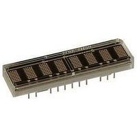
Manufacturer Part Number
HCMS-2914
Description
LED DISPLAY 5X7 8CHAR 3.8MM ORN
Manufacturer
Avago Technologies US Inc.
Series
HCMS-29xxr
Datasheet
1.HCMS-2903.pdf
(16 pages)
Specifications of HCMS-2914
Millicandela Rating
*
Size / Dimension
1.40" L x 0.40" W x 0.20" H (35.6mm x 10.2mm x 5.1mm)
Color
Orange
Configuration
5 x 7
Voltage - Forward (vf) Typ
*
Package / Case
26-DIP
Display Type
Alphanumeric
Number Of Digits/alpha
8
Digit/alpha Size
0.15" (3.8mm)
Character Format
Dot Matrix
Character Size
3.81mm
Led Color
Orange
Luminous Intensity
64µcd
No. Of Digits / Alpha
8
Display Area Width
35.56mm
Display Area Height
10.16mm
Number Of Digits
8
Illumination Color
Orange
Wavelength
600 nm
Operating Voltage
- 0.3 V to 5.5 V
Maximum Operating Temperature
+ 85 C
Minimum Operating Temperature
- 40 C
Lead Free Status / RoHS Status
Lead free / RoHS Compliant
Common Pin
-
Lead Free Status / Rohs Status
Details


Display Overview
The HCMS-29xx series is a family of LED displays driven
by on-board CMOS ICs. The LEDs are configured as 5 x 7
font characters and are driven in groups of 4 characters
per IC. Each IC consists of a 160-bit shift register (the Dot
Register), two 7-bit Control Words, and refresh circuitry.
The Dot Register contents are mapped on a one-to-one
basis to the display. Thus, an individual Dot Register bit
uniquely controls a single LED.
8-character displays have two ICs that are cascaded. The
Data Out line of the first IC is internally connected to
the Data In line of the second IC forming a 320-bit Dot
Register. The display’s other control and power lines are
connected directly to both ICs. In 16-character displays,
each row functions as an independent 8-character display
with its own 320-bit Dot Register.
Reset
Reset initializes the Control Registers (sets all Control
Register bits to logic low) and places the display in the
sleep mode. The Reset pin should be connected to the
system power-on reset circuit. The Dot Registers are not
cleared upon power-on or by Reset. After power-on, the
Dot Register contents are random; however, Reset will
put the display in sleep mode, thereby blanking the
LEDs. The Control Register and the Control Words are
cleared to all zeros by Reset.
To operate the display after being Reset, load the Dot
Register with logic lows. Then load Control Word 0 with
the desired brightness level and set the sleep mode bit
to logic high.
Table 1. Register Truth Table
Function
Select Dot Register
Load Dot Register
D
D
Copy Data from Dot Register to Dot Latch
Select Control Register
Load Control Register
Latch Data to
Notes:
1. BIT D
2. Selection of Control Word 1 or Control Word 0 is set by D
3. Control Word data is loaded Most Significant Bit (D
8
ous mode.
ed control word retains its previous value.
IN
IN
0
of Control Word 1 must have been previously set to Low for serial mode or High for simultane-
= HIGH LED = “ON”
= LOW LED = “OFF”
Control Word
[1,3]
[2]
7
) first.
7
of the Control Shift Register. The unselect-
↑ ↓
↑ ↓
CLK
Not Rising
L
Not Rising
L
Dot Register
The Dot Register holds the pattern to be displayed by
the LEDs. Data is loaded into the Dot Register according
to the procedure shown in Table 1 and the Write Cycle
Timing Diagram.
First RS is brought low, then CE is brought low. Next,
each successive rising CLK edge will shift in the data
at the D
responding LED on; a logic low turns the LED off. When
all 160 bits have been loaded (or 320 bits in an 8-digit
display), CE is brought to logic high.
When CLK is next brought to logic low, new data is
latched into the display dot drivers. Loading data into
the Dot Register takes place while the previous data is
displayed and eliminates the need to blank the display
while loading data.
Pixel Map
In a 4-character display, the 160-bits are arranged as 20
columns by 8 rows. This array can be conceptualized as
four 5 x 8 dot matrix character locations, but only 7 of
the 8 rows have LEDs (see Figures 1 & 2). The bottom
row (row 0) is not used. Thus, latch location 0 is never
displayed. Column 0 controls the left-most column. Data
from Dot Latch locations 0-7 determine whether or not
pixels in Column 0 are turned-on or turned-off. Therefore,
the lower left pixel is turned-on when a logic high is
stored in Dot Latch location 1. Characters are loaded
in serially, with the left-most character being loaded
first and the right-most character being loaded last. By
loading one character at a time and latching the data
before loading the next character, the figures will appear
to scroll from right to left.
↑ ↓
↑ ↓
IN
CE
H
L
↑ ↓
L
pin. Loading a logic high will turn the cor-
RS
L
X
X
H
X
X
Related parts for HCMS-2914
Image
Part Number
Description
Manufacturer
Datasheet
Request
R

Part Number:
Description:
LED DISPLAY 5X7 4CHAR 5MM GREEN
Manufacturer:
Avago Technologies US Inc.
Datasheet:

Part Number:
Description:
LED DISPLAY 5X7 8CHAR 3.8MM YLW
Manufacturer:
Avago Technologies US Inc.
Datasheet:

Part Number:
Description:
LED DISPLAY 5X7 4CHAR 3.8MM YLW
Manufacturer:
Avago Technologies US Inc.
Datasheet:

Part Number:
Description:
LED DISPLAY 5X7 4CHAR 3.8MM ORN
Manufacturer:
Avago Technologies US Inc.
Datasheet:

Part Number:
Description:
LED DISPL 5X7 4CHAR 3.8MM ALGAAS
Manufacturer:
Avago Technologies US Inc.
Datasheet:
Part Number:
Description:
LED DISPLAY 5X7 4CHAR 3.8MM RED
Manufacturer:
Avago Technologies US Inc.
Datasheet:
Part Number:
Description:
LED DISPLAY 5X7 4CHAR 3.8MM ORN
Manufacturer:
Avago Technologies US Inc.
Datasheet:
Part Number:
Description:
LED DISPLAY 5X7 4CHAR 3.8MM YLW
Manufacturer:
Avago Technologies US Inc.
Datasheet:
Part Number:
Description:
LED DISPLAY 5X7 4CHAR 5MM YLW
Manufacturer:
Avago Technologies US Inc.
Datasheet:
Part Number:
Description:
LED DISPLAY 5X7 4CHAR 5MM ORN
Manufacturer:
Avago Technologies US Inc.
Datasheet:
Part Number:
Description:
LED DISPLAY 5X7 4CHAR 5MM GRN
Manufacturer:
Avago Technologies US Inc.
Datasheet:
Part Number:
Description:
LED DISPLAY 5X7 4CHAR 5MM RED
Manufacturer:
Avago Technologies US Inc.
Datasheet:
Part Number:
Description:
LED DISPLAY 5X7 4CHAR 3.8MM RED
Manufacturer:
Avago Technologies US Inc.
Datasheet:
Part Number:
Description:
LED DISPLAY 5X7 4CHAR 3.8MM GRN
Manufacturer:
Avago Technologies US Inc.
Datasheet:
Part Number:
Description:
LED DISPLAY 5X7 4CHAR 5MM GRN
Manufacturer:
Avago Technologies US Inc.
Datasheet: