HCMS-2965 Avago Technologies US Inc., HCMS-2965 Datasheet - Page 15
HCMS-2965
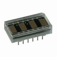
Manufacturer Part Number
HCMS-2965
Description
LED DISPLAY 5X7 4CHAR .2" RED
Manufacturer
Avago Technologies US Inc.
Series
HCMS-29xxr
Datasheet
1.HCMS-2903.pdf
(16 pages)
Specifications of HCMS-2965
Display Type
Alphanumeric
Millicandela Rating
*
Internal Connection
*
Size / Dimension
0.85" L x 0.45" W x 0.21" H (21.5mm x 11.4mm x 5.3mm)
Color
Red
Configuration
*
Voltage - Forward (vf) Typ
*
Package / Case
12-DIP
Number Of Digits/alpha
4
Digit/alpha Size
0.20" (5mm)
Number Of Digits
4
Character Size
2.54 mm x 4.57 mm
Illumination Color
Red
Wavelength
637 nm
Operating Voltage
5 V
Operating Current
10 mA
Maximum Operating Temperature
+ 85 C
Minimum Operating Temperature
- 40 C
Luminous Intensity
230 ucd
Power Consumption
1.2 W
Viewing Area (w X H)
18.62 mm x 4.57 mm
Common Pin
None
Lead Free Status / RoHS Status
Lead free / RoHS Compliant
Lead Free Status / RoHS Status
Lead free / RoHS Compliant, Lead free / RoHS Compliant
Other names
516-1606-5


Current Calculations
The peak and average display current requirements have
a significant impact on power supply selection. The
maximum peak current is calculated with Equation 3.
The average current required by the display can be
calculated with Equation 4.
The power supply has to be able to supply I
sients and supply I
V
changing the display brightness.
V
The display uses two independent electrical systems.
One system is used to power the display’s logic and the
other to power the display’s LEDs. These two systems
keep the logic supply clean.
Separate electrical systems allow the voltage applied
to V
V
the Dot or the Control Registers. V
between 4.0 to 5.5 V without any noticeable variation in
light output. However, operating V
cause objectionable mismatch between the pixels and is
not recommended. Dimming the display by pulse width
modulating V
V
the displayed message or the display intensity. However,
operation below 4.5 V will change the timing and logic
levels and operation below 3 V may cause the Dot and
Control Registers to be altered.
The logic ground is internally connected to the LED
ground by a substrate diode. This diode becomes for-
ward biased and conducts when the logic ground is 0.4
V greater than the LED ground. The LED ground and
the logic ground should be connected to a common
ground which can withstand the current introduced by
the switching LED drivers. When separate ground con-
nections are used, the LED ground can vary from -0.3
V to +0.3 V with respect to the logic ground. Voltages
below -0.3 V can cause all the dots to be ON. Voltage
above +0.3 V can cause dimming and dot mismatch. The
LED ground for the LED drivers can be routed separately
from the logic ground until an appropriate ground
plane is available. On long interconnections between
the display and the host system, voltage drops on the
analog ground can be kept from affecting the display
logic levels by isolating the two grounds.
15
LED
LOGIC
LED
LOGIC
allows noise on this supply without significantly
LED
can vary from 0 to 5.5 V without affecting either
and V
can vary from 3.0 to 5.5 V without affecting either
and V
LED
LED
LOGIC
Considerations
is also not recommended.
LED
to be varied independently. Thus,
(AVG) continuously. The range on
LED
LED
below 4.0 V may
can be varied
PEAK
tran-
Electrostatic Discharge
The inputs to the ICs are protected against static dis-
charge and input current latchup. However, for best
results, standard CMOS handling precautions should
be used. Before use, the HCMS-29XX should be stored
in antistatic tubes or in conductive material. During
assembly, a grounded conductive work area should be
used and assembly personnel should wear conductive
wrist straps. Lab coats made of synthetic material should
be avoided since they are prone to static buildup. In-
put current latchup is caused when the CMOS inputs
are subjected to either a voltage below ground (V
ground) or to a voltage higher than V
and when a high current is forced into the input. To
prevent input current latchup and ESD damage, unused
inputs should be connected to either ground or V
Voltages should not be applied to the inputs until V
has been applied to the display.
Appendix C. Oscillator
The oscillator provides the internal refresh circuitry with
a signal that is used to synchronize the columns and
rows. This ensures that the right data is in the dot driv-
ers for that row. This signal can be supplied from either
an external source or the internal source.
A display refresh rate of 100 Hz or faster ensures
flicker-free operation. Thus for an external oscillator
the frequency should be greater than or equal to 512
x 100 Hz = 51.2 kHz. Operation above 1 MHz without
the prescaler or 8 MHz with the prescaler may cause
noticeable pixel to pixel mismatch.
Appendix D. Refresh Circuitry
This display driver consists of 20 one-of-eight column
decoders and 20 constant current sources, 1 one-of-eight
row decoder and eight row sinks, a pulse width modula-
tion control block, a peak current control block, and the
circuit to refresh the LEDs. The refresh counters and oscil-
lator are used to synchronize the columns and rows.
The 160 bits are organized as 20 columns by 8 rows. The
IC illuminates the display by sequentially turning ON each
of the 8 row-drivers. To refresh the display once takes
512 oscillator cycles. Because there are eight row driv-
ers, each row driver is selected for 64 (512/8) oscillator
cycles. Four cycles are used to briefly blank the display
before the following row is switched on. Thus, each row
is ON for 60 oscillator cycles out of a possible 64. This
corresponds to the maximum LED on time.
LOGIC
(V
IN
> V
LOGIC
LOGIC
LOGIC
IN
<
)
.
Related parts for HCMS-2965
Image
Part Number
Description
Manufacturer
Datasheet
Request
R

Part Number:
Description:
LED DISPLAY 5X7 4CHAR 5MM GREEN
Manufacturer:
Avago Technologies US Inc.
Datasheet:

Part Number:
Description:
LED DISPLAY 5X7 8CHAR 3.8MM YLW
Manufacturer:
Avago Technologies US Inc.
Datasheet:

Part Number:
Description:
LED DISPLAY 5X7 4CHAR 3.8MM YLW
Manufacturer:
Avago Technologies US Inc.
Datasheet:

Part Number:
Description:
LED DISPLAY 5X7 4CHAR 3.8MM ORN
Manufacturer:
Avago Technologies US Inc.
Datasheet:

Part Number:
Description:
LED DISPL 5X7 4CHAR 3.8MM ALGAAS
Manufacturer:
Avago Technologies US Inc.
Datasheet:
Part Number:
Description:
LED DISPLAY 5X7 4CHAR 3.8MM RED
Manufacturer:
Avago Technologies US Inc.
Datasheet:
Part Number:
Description:
LED DISPLAY 5X7 4CHAR 3.8MM ORN
Manufacturer:
Avago Technologies US Inc.
Datasheet:
Part Number:
Description:
LED DISPLAY 5X7 4CHAR 3.8MM YLW
Manufacturer:
Avago Technologies US Inc.
Datasheet:
Part Number:
Description:
LED DISPLAY 5X7 4CHAR 5MM YLW
Manufacturer:
Avago Technologies US Inc.
Datasheet:
Part Number:
Description:
LED DISPLAY 5X7 4CHAR 5MM ORN
Manufacturer:
Avago Technologies US Inc.
Datasheet:
Part Number:
Description:
LED DISPLAY 5X7 4CHAR 5MM GRN
Manufacturer:
Avago Technologies US Inc.
Datasheet:
Part Number:
Description:
LED DISPLAY 5X7 4CHAR 5MM RED
Manufacturer:
Avago Technologies US Inc.
Datasheet:
Part Number:
Description:
LED DISPLAY 5X7 4CHAR 3.8MM RED
Manufacturer:
Avago Technologies US Inc.
Datasheet:
Part Number:
Description:
LED DISPLAY 5X7 4CHAR 3.8MM GRN
Manufacturer:
Avago Technologies US Inc.
Datasheet:
Part Number:
Description:
LED DISPLAY 5X7 4CHAR 5MM GRN
Manufacturer:
Avago Technologies US Inc.
Datasheet: