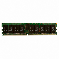
MT72HTS1G72PY-53EE1 Micron Technology Inc, MT72HTS1G72PY-53EE1 Datasheet

MT72HTS1G72PY-53EE1
Specifications of MT72HTS1G72PY-53EE1
Related parts for MT72HTS1G72PY-53EE1
MT72HTS1G72PY-53EE1 Summary of contents
Page 1
DDR2 SDRAM RDIMM MT72HT(Z)S1G72P – 8GB For the latest component data sheets, refer to Micron’s Web site: Features • 240-pin, registered dual in-line memory module (RDIMM) ™ • Quad rank, using 36 TwinDie • Fast data transfer rates: PC2-3200, PC2-4200, ...
Page 2
... Notes: 1. Data sheets for the base device can be found on Micron’s Web site. 2. All part numbers end with a two-place code (not shown), designating component and PCB revisions. Consult factory for current revision codes. Example: MT72HTS1G72PY-667E1. PDF: 09005aef82d283a8/Source: 09005aef82d28271 HTS72C1Gx72.fm - Rev. A 8/07 EN ...
Page 3
Pin Assignments and Descriptions Table 4: Pin Assignments 240-Pin RDIMM Front Pin Symbol Pin Symbol Pin Symbol Pin Symbol DQ19 61 REF DQ0 33 DQ24 63 4 DQ1 34 ...
Page 4
Table 5: Pin Descriptions Symbol Type Description A0–A15 Input Address inputs: Provide the row address for ACTIVE commands, and the column address (SSTL_18) and auto precharge bit (A10) for READ/WRITE commands, to select one location out of the memory array ...
Page 5
Functional Block Diagram Figure 2: Functional Block Diagram V SS RS3# RS2# RS1# RS0# DQS0 DQS0# DM CS# DQS DQS# DM CS# DQS DQS# DQ DQ0 DQ1 DQ2 DQ DQ DQ3 DQ ...
Page 6
... READs and by the memory controller during WRITEs. DQS is edge- aligned with data for READs and center-aligned with data for WRITEs. DDR2 SDRAM modules operate from a differential clock (CK and CK#); the crossing of CK going HIGH and CK# going LOW will be referred to as the positive edge of CK. ...
Page 7
... Simulations are significantly more accurate and realistic than a gross estimation of module capacitance when inductance and delay parameters associated with trace lengths are used in simulations. JEDEC modules are currently designed using simulations to close timing budgets. Component Timing and Operating Conditions Recommended AC operating conditions are given in the DDR2 component data sheets. Component specifications are available on Micron’ ...
Page 8
I Specifications DD Table 8: DDR2 I Specifications and Conditions – 8GB DD Values are shown for the MT47H512M4THN DDR2 SDRAM only and are computed from values specified in the MT47H256M4 2Gb TwinDie™ component data sheet Parameter/Condition Operating one bank ...
Page 9
Register and PLL Specifications Table 9: Register Specifications SSTU32868 devices or equivalent JESD82-14 Parameter Symbol high-level IH DC input voltage DC low-level input voltage AC high-level ...
Page 10
Table 10: PLL Specifications CU877 device or equivalent JESD82-8.01 Parameter Symbol DC high-level input V IH voltage DC low-level input V IL voltage V Input voltage (limits high-level input V IH voltage V DC low-level input IL voltage ...
Page 11
Serial Presence-Detect Table 12: Serial Presence-Detect EEPROM DC Operating Conditions Parameter/Condition Supply voltage Input high voltage: Logic 1; All inputs Input low voltage: Logic 0; All inputs Output low voltage 3mA OUT Input leakage current GND ...
Page 12
Table 14: Serial Presence-Detect Matrix Byte Description 0 Number of SPD bytes used by Micron 1 Total number of bytes in SPD device 2 Fundamental memory type 3 Number of row addresses on SDRAM 4 Number of column addresses on ...
Page 13
Table 14: Serial Presence-Detect Matrix (continued) Byte Description 33 Address and command hold time, 34 Data/data mask input setup time, 35 Data/data mask input hold time Write recovery time WRITE-to-READ command delay, 38 READ-to-PRECHARGE command delay, ...
Page 14
Module Dimensions Figure 3: 240-Pin DDR2 RDIMM 2.0 (0.079 (4X) U11 U12 U13 2.5 (0.098) D (2X) 2.3 (0.091) TYP Pin 1 1.0 (0.039) 2.21 (0.087) TYP TYP 1.0 (0.039) TYP 70.66 (2.782) TYP U21 U22 ...
Page 15
Figure 4: 240-Pin DDR2 RDIMM with Heat Spreader 2.0 (0.079 (4X) U11 U12 U13 2.50 (0.098) D (2X) 2.30 (0.091) TYP Pin 1 2.21 (0.087) TYP 1.0 (0.039) TYP 1.0 (0.039) TYP 70.66 (2.782) TYP U21 ...


