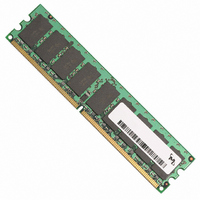
MT9HTF6472AY-800D1 Micron Technology Inc, MT9HTF6472AY-800D1 Datasheet - Page 36

MT9HTF6472AY-800D1
Manufacturer Part Number
MT9HTF6472AY-800D1
Description
MODULE DDR2 512MB 240-DIMM
Manufacturer
Micron Technology Inc
Datasheet
1.MT9HTF12872AY-40ED1.pdf
(44 pages)
Specifications of MT9HTF6472AY-800D1
Memory Type
DDR2 SDRAM
Memory Size
512MB
Speed
800MT/s
Package / Case
240-DIMM
Lead Free Status / RoHS Status
Lead free / RoHS Compliant
pdf: 09005aef80e6f860, source: 09005aef80e5b799
HTF9C32_64_128x72AG_2.fm - Rev. C 6/05 EN
13. It is recommended that DQS be valid (HIGH or LOW) on or before the WRITE com-
14. The refresh period is 64ms. This equates to an average refresh rate of 7.8125µs. How-
15. Each byte lane has a corresponding DQS.
16. CK and CK# input slew rate must be ≥ 1V/ns (≥ 2 V/ns if measured differentially).
17. The data valid window is derived by achieving other specifications -
18.
19. MIN(
20.
21. READs and WRITEs with auto precharge are allowed to be issued before
22. V
23.
24. The minimum READ to internal PRECHARGE time. This parameter is only applicable
25. Operating frequency is only allowed to change during self refresh mode, precharge
26. ODT turn-on time
27. ODT turn-off time
28. This parameter has a two clock minimum requirement at any
29.
30.
31. No more than 4 bank ACTIVE commands may be issued in a given
mand. The case shown (DQS going from High-Z to logic LOW) applies when no
WRITEs were previously in progress on the bus. If a previous WRITE was in progress,
DQS could be HIGH during this time, depending on
ever, a REFRESH command must be asserted at least once every 70.3µs or
(MAX). To ensure all rows of all banks are properly refreshed, 8192 REFRESH com-
mands must be issued every 64ms.
t
tion to the clock duty cycle and a practical data valid window can be derived.
t
high time as provided to the device (i.e. This value can be greater than the minimum
specification limits for
period, less the half period jitter [
jitter due to cross talk [
t
device CK and CK# inputs.
satisfied since
SDRAM data sheet for more detail.
t
round to the next highest integer.
refers to the
ns with
clocks = 8 clocks.
when
standing,
matically delay the internal PRECHARGE command until
satisfied.
power-down mode, and system reset condition.
resistance begins to turn on. ODT turn-on time
tance is fully on. Both are measured from
ODT turn off time
sured from
t
prior to CK, CK# being removed in a system RESET condition.
t
t
DDR2 devices, regardless of the number of banks already open or closed.
DQSQ, and
JIT specification is currently TBD.
HP (MIN) is the lesser of
DAL = (nWR) + (
DELAY is calculated from
ISXR is equal to
RRD(min) restriction still applies. The
256MB, 512MB, 1GB (x72, SR, ECC) 240-Pin DDR2 SDRAM UDIMM
IL
/V
t
IH
CL,
t
RTP/(2*
t
DDR2 overshoot/undershoot. R
WR programmed to four clocks.
t
t
CH) refers to the smaller of the actual clock low time and the actual clock
RAS (MIN) has to be satisfied as well. The DDR2 SDRAM device will auto-
t
AOFD.
t
t
WR parameter stored in the MR[11,10,9]. Example: For -53E at
QH (
t
t
RAS lockout feature is supported in DDR2 SDRAM devices.
CK) > 1. If
t
IS and is used for CKE setup time during self refresh exit.
t
t
QH =
RP/
t
t
t
AOF (MAX) is when the bus is in high impedance. Both are mea-
AON (MIN) is when the device leaves high impedance and ODT
AOF (MIN) is when the device starts to turn off ODT resistance.
t
t
t
JIT(cross talk)] into the clock traces.
CK): For each of the terms above, if not already an integer,
CL and
t
HP -
t
RTP/(2*
t
36
t
IS +
CL minimum and
t
QHS). The data valid window derates in direct propor-
t
CH). For example,
t
CK +
t
JIT(HP)] of the clock source, and less the half period
t
CK) ≤ 1, then equation AL + BL/2 applies. Notwith-
t
Micron Technology, Inc., reserves the right to change products or specifications without notice.
CK refers to the application clock period; nWR
t
IH so that CKE registration LOW is guaranteed
t
EFER TO
FAW(min) parameter applies to all 8 bank
t
AOND.
t
DAL = 4 + (15 ns/3.75 ns) clocks = 4 +(4)
t
CH minimum actually applied to the
t
AON (MAX) is when the ODT resis-
the 256Mb, 512Mb, or 1Gb DDR2
t
CL and
t
DQSS.
©2003, 2004, 2005 Micron Technology, Inc. All rights reserved.
t
CH are = 50 percent of the
t
CK.
t
RAS (MIN) has been
t
FAW(min) period.
t
RAS (MIN) is
t
HP . (
t
CK = 3.75
Notes
t
CK/2),
t
RFC


