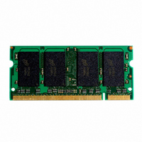
MT4LSDT864HG-133G2 Micron Technology Inc, MT4LSDT864HG-133G2 Datasheet - Page 7

MT4LSDT864HG-133G2
Manufacturer Part Number
MT4LSDT864HG-133G2
Description
MODULE SDRAM 64MB 144SODIMM
Manufacturer
Micron Technology Inc
Datasheet
1.MT4LSDT864HG-133G2.pdf
(22 pages)
Specifications of MT4LSDT864HG-133G2
Memory Type
SDRAM
Memory Size
64MB
Speed
133MHz
Package / Case
144-SODIMM
Main Category
DRAM Module
Sub-category
SDRAM
Module Type
144SODIMM
Device Core Size
64b
Organization
8Mx64
Total Density
64MByte
Chip Density
128Mb
Access Time (max)
6/5.4ns
Maximum Clock Rate
133MHz
Operating Supply Voltage (typ)
3.3V
Operating Current
600mA
Number Of Elements
4
Operating Supply Voltage (max)
3.6V
Operating Supply Voltage (min)
3V
Operating Temp Range
0C to 65C
Operating Temperature Classification
Commercial
Pin Count
144
Mounting
Socket
Lead Free Status / RoHS Status
Contains lead / RoHS non-compliant
General Description
MT4LSDT1664H are high-speed CMOS, dynamic ran-
dom-access 32MB, 64MB, and 128MB unbuffered
memory modules, organized in x64 configurations.
These modules use internally configured quad-bank
SDRAMs with a synchronous interface (all signals are
registered on the positive edge of the clock signal CK).
burst oriented; accesses start at a selected location and
continue for a programmed number of locations in a
programmed sequence. Accesses begin with the regis-
tration of an ACTIVE command, which is then fol-
lowed by a READ or WRITE command. The address
bits registered coincident with the ACTIVE command
are used to select the device bank and row to be
accessed (BA0, BA1 select the device bank, A0–A11
[32MB and 64MB], or A0–A12 [128MB] select the
device row). The address bits A0–A7 (32MB), or A0–A8
(64MB and 128MB), registered coincident with the
READ or WRITE command, are used to select the start-
ing device column location for the burst access.
WRITE burst lengths of 1, 2, 4, or 8 locations, or the full
page, with a burst terminate option. An auto precharge
function may be enabled to provide a self-timed row
precharge that is initiated at the end of the burst
sequence.
ture to achieve high-speed operation. This architec-
ture is compatible with the 2n rule of prefetch
architectures, but it also allows the column address to
be changed on every clock cycle to achieve a high-
speed, fully random access. Precharging one device
bank while accessing one of the other three device
banks will hide the precharge cycles and provide
seamless, high-speed, random-access operation.
power memory systems. An auto refresh mode is pro-
vided, along with a power-saving, power-down mode.
All inputs and outputs are LVTTL-compatible.
DRAM operating performance, including the ability to
synchronously burst data at a high data rate with auto-
matic column-address generation, the ability to inter-
leave between internal banks in order to hide
precharge time and the capability to randomly change
column addresses on each clock cycle during a burst
access. For more information regarding SDRAM oper-
ation, refer to the 64Mb, 128Mb, or 256Mb SDRAM
component data sheets.
09005aef80748a77
SD4C4_8_16X64HG.fm - Rev. C 6/04 EN
The Micron MT4LSDT464H, MT4LSDT864H, and
Read and write accesses to the SDRAM modules are
These modules provide for programmable READ or
These modules use an internal pipelined architec-
These modules are designed to operate in 3.3V, low-
SDRAM modules offer substantial advances in
7
Serial Presence Detect Operation
(SPD).
2,048-bit EEPROM. This nonvolatile storage device
contains 256 bytes.
grammed by Micron to identify the module type,
SDRAM characteristics and module timing parame-
ters. The remaining 128 bytes of storage are available
for use by the customer. System READ/WRITE opera-
tions between the master (system logic) and the slave
EEPROM device (DIMM) occur via a standard I
using the DIMM’s SCL (clock) and SDA (data) signals,
together with SA(2:0), which provide eight unique
DIMM/EEPROM addresses. Write protect (WP) is tied
to ground on the module, permanently disabling hard-
ware write protect.
Initialization
predefined manner.
than those specified may result in undefined opera-
tion. Once power is applied to V
taneously) and the clock is stable (stable clock is
defined as a signal cycling within timing constraints
specified for the clock pin), the SDRAM requires a
100µs delay prior to issuing any command other than a
COMMAND INHIBIT or NOP . Starting at some point
during this 100µs period and continuing at least
through the end of this period, COMMAND INHIBIT
or NOP commands should be applied.
one COMMAND INHIBIT or NOP command having
been applied, a PRECHARGE command should be
applied. All device banks must then be precharged,
thereby placing the device in the all banks idle state.
must be performed. After the AUTO REFRESH cycles
are complete, the SDRAM is ready for mode register
programming. Because the mode register will power
up in an unknown state, it should be loaded prior to
applying any operational command.
Mode Register Definition
mode of operation of the SDRAM. This definition
includes the selection of a burst length, a burst type, a
CAS latency, an operating mode, and a write burst
mode, as shown in Figure 4, Mode Register Definition
Diagram, on page 8. The mode register is programmed
via the LOAD MODE REGISTER command and will
retain the stored information until it is programmed
again or the device loses power.
These modules incorporate serial presence-detect
SDRAMs must be powered up and initialized in a
Once the 100µs delay has been satisfied with at least
Once in the idle state, two AUTO REFRESH cycles
The mode register is used to define the specific
32MB, 64MB, 128MB (x64, SR)
Micron Technology, Inc., reserves the right to change products or specifications without notice.
The SPD function is implemented using a
144-PIN SDRAM SODIMM
Operational procedures other
The first 128 bytes are pro-
©2004 Micron Technology, Inc. All rights reserved.
DD
and V
DD
Q (simul-
2
C bus


