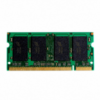
MT16VDDF12864HG-335F2 Micron Technology Inc, MT16VDDF12864HG-335F2 Datasheet - Page 10

MT16VDDF12864HG-335F2
Manufacturer Part Number
MT16VDDF12864HG-335F2
Description
MODULE DDR SDRAM 1GB 200-SODIMM
Manufacturer
Micron Technology Inc
Datasheet
1.MT16VDDF12864HY-335F2.pdf
(30 pages)
Specifications of MT16VDDF12864HG-335F2
Memory Type
DDR SDRAM
Memory Size
1GB
Speed
333MT/s
Package / Case
200-SODIMM
Lead Free Status / RoHS Status
Contains lead / RoHS non-compliant
Table 6:
NOTE:
Table 7:
pdf: 09005aef80a77a90, source: 09005aef80a646bc
DDF16C64_128x64HG.fm - Rev. D 9/04 EN
1. For a burst length of two, A1-Ai select the two-data-ele-
2. For a burst length of four, A2-Ai select the four-data-
3. For a burst length of eight, A3-Ai select the eight-data-
4. Whenever a boundary of the block is reached within a
5. i = 9 (512MB);
LENGTH
BURST
ment block; A0 selects the first access within the block.
element block; A0-A1 select the first access within the
block.
element block; A0-A2 select the first access within the
block.
given sequence above, the following access wraps
within the block.
i = 9,11 (1GB)
2
4
8
SPEED
-26A
-335
-262
-265
A2 A1 A0
0
0
0
0
1
1
1
1
STARTING
ADDRESS
COLUMN
Burst Definition Table
CAS Latency (CL) Table
A1 A0
0
0
1
1
0
0
1
1
0
0
1
1
A0
0
1
0
1
0
1
0
1
0
1
0
1
0
1
75
75
75
75
CLOCK FREQUENCY (MHZ)
CL = 2
ALLOWABLE OPERATING
ORDER OF ACCESSES WITHIN
0-1-2-3-4-5-6-7
1-2-3-4-5-6-7-0
2-3-4-5-6-7-0-1
3-4-5-6-7-0-1-2
4-5-6-7-0-1-2-3
5-6-7-0-1-2-3-4
6-7-0-1-2-3-4-5
7-0-1-2-3-4-5-6
SEQUENTIAL
f
f
f
f
133
133
133
100
TYPE =
0-1-2-3
1-2-3-0
2-3-0-1
3-0-1-2
0-1
1-0
A BURST
75
75
75
75
INTERLEAVED
0-1-2-3-4-5-6-7
1-0-3-2-5-4-7-6
2-3-0-1-6-7-4-5
3-2-1-0-7-6-5-4
4-5-6-7-0-1-2-3
5-4-7-6-1-0-3-2
6-7-4-5-2-3-0-1
7-6-5-4-3-2-1-0
CL = 2.5
TYPE =
0-1-2-3
1-0-3-2
2-3-0-1
3-2-1-0
f
f
f
f
0-1
1-0
167
133
133
133
10
reserved for future use and/or test modes. Test modes
and reserved states should not be used because
unknown operation or incompatibility with future ver-
sions may result.
Extended Mode Register
beyond those controlled by the mode register; these
additional functions are DLL enable/disable and out-
put drive strength. These functions are controlled via
the bits shown in Figure 7, Extended Mode Register
Definition Diagram, on page 11. The extended mode
register is programmed via the LOAD MODE REGIS-
TER command to the mode register (with BA0 = 1 and
BA1 = 0) and will retain the stored information until it
is programmed again or the device loses power. The
enabling of the DLL should always be followed by a
LOAD MODE REGISTER command to the mode regis-
ter (BA0/ BA1 both LOW) to reset the DLL.
all device banks are idle and no bursts are in progress,
and the controller must wait the specified time before
initiating any subsequent operation. Violating either of
these requirements could result in unspecified opera-
tion.
COMMAND
COMMAND
All other combinations of values for A7–A12 are
The extended mode register controls functions
The extended mode register must be loaded when
DQS
DQS
CK#
CK#
DQ
DQ
Micron Technology, Inc., reserves the right to change products or specifications without notice.
Figure 6: CAS Latency Diagram
CK
CK
READ
READ
Burst Length = 4 in the cases shown
Shown with nominal t AC, t DQSCK, and t DQSQ
T0
T0
200-PIN DDR SODIMM
512MB, 1GB (x64, DR)
CL = 2
TRANSITIONING DATA
CL = 2.5
NOP
NOP
T1
T1
T2
NOP
NOP
T2
©2004 Micron Technology, Inc.
T2n
T2n
DON T CARE
T3
NOP
NOP
T3
T3n
T3n


