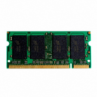
MT18VDDF12872HG-40BD1 Micron Technology Inc, MT18VDDF12872HG-40BD1 Datasheet - Page 14

MT18VDDF12872HG-40BD1
Manufacturer Part Number
MT18VDDF12872HG-40BD1
Description
MODULE DDR SDRAM 1GB 200-SODIMM
Manufacturer
Micron Technology Inc
Datasheet
1.MT18VDDF12872HY-40BF1.pdf
(26 pages)
Specifications of MT18VDDF12872HG-40BD1
Memory Type
DDR SDRAM
Memory Size
1GB
Speed
200MHz
Package / Case
200-SODIMM
Lead Free Status / RoHS Status
Contains lead / RoHS non-compliant
Other names
557-1116
Table 13: Capacitance
Note: 11; notes appear notes appear on pages 16–18
Table 14: DDR SDRAM Component Electrical Characteristics and
Notes: 1–5, 12–15, 28; notes appear on pages 16–18; 0°C
pdf: 09005aef80e4880c, source: 09005aef80e487d7
DDAF18C128x72HG.fm - Rev. A 10/04 EN
PARAMETER
Input/Output Capacitance: DQ, DQS,DM
Input Capacitance: Command and Address
Input Capacitance: CK, CK#,
Input Capacitance: CKE, S#
AC CHARACTERISTICS
PARAMETER
Access window of DQs from CK/CK#
CK high-level width
CK low-level width
Clock cycle time
DQ and DM input hold time relative to DQS
DQ and DM input setup time relative to DQS
DQ and DM input pulse width (for each input)
Access window of DQS from CK/CK#
DQS input high pulse width
DQS input low pulse width
DQS-DQ skew, DQS to last DQ valid, per group, per access
Write command to first DQS latching transition
DQS falling edge to CK rising - setup time
DQS falling edge from CK rising - hold time
Half clock period
Data-out high-impedance window from CK/CK#
Data-out low-impedance window from CK/CK#
Address and control input hold time (1 V/ns)
Address and control input setup time (1 V/ns)
Address and control input hold time (0.5 V/ns)
Address and control input setup time (0.5 V/ns)
Address and Control input pulse width (for each input)
LOAD MODE REGISTER command cycle time
DQ-DQS hold, DQS to first DQ to go non-valid, per access
Data hold skew factor
ACTIVE to PRECHARGE command
ACTIVE to READ with Auto precharge command
ACTIVE to ACTIVE/AUTO REFRESH command period
AUTO REFRESH command period
Recommended AC Operating Conditions
CL = 3
CL = 2.5
CL = 2
T
A
14
SYMBOL
t
t
CK (2.5)
t
t
t
t
t
DQSCK
t
t
t
CK (3)
CK (2)
DQSH
DQSQ
+70°C; V
DIPW
t
t
DQSL
DQSS
t
t
t
t
MRD
t
t
t
t
t
DSH
t
t
t
t
QHS
RAP
t
IPW
RAS
t
t
DSS
t
t
t
RFC
QH
DH
AC
CH
HP
HZ
IH
IH
CL
DS
RC
LZ
IS
IS
F
S
F
S
Micron Technology, Inc., reserves the right to change products or specifications without notice.
DD
t
HP -
= V
1GB (x72, ECC, DR) PC3200
-0.70
MIN
0.45
0.45
1.75
0.35
0.35
0.72
2.20
-0.7
-0.6
7.5
0.4
0.4
0.2
0.2
0.6
0.6
0.6
0.6
40
15
55
70
5
6
2
DD
t
SYMBOL
QHS
Q = +2.6V ±0.1V
t
C
C
C
C
CH,
-40B
IO
200-PIN DDR SODIMM
I1
I2
I3
t
CL
70,000
MAX
+0.70
+0.7
0.55
0.55
+0.6
0.40
1.28
0.50
7.5
13
13
MIN
13.5
27
7
9
UNITS
t
t
t
t
t
t
t
ns
CK
CK
ns
ns
ns
ns
ns
ns
ns
CK
CK
ns
CK
CK
CK
ns
ns
ns
ns
ns
ns
ns
ns
ns
ns
ns
ns
ns
ns
ns
MAX
©2004 Micron Technology, Inc.
45
15
22
9
NOTES
39, 44
39, 44
23, 27
23, 27
22, 23
16, 36
16, 36
UNITS
25
25
27
22
29
12
12
12
12
30
42
44
22
pF
pF
pF
pF


