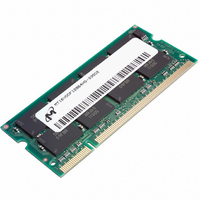
MT16VDDF12864HG-335D2 Micron Technology Inc, MT16VDDF12864HG-335D2 Datasheet - Page 20

MT16VDDF12864HG-335D2
Manufacturer Part Number
MT16VDDF12864HG-335D2
Description
MODULE DDR SDRAM 1GB 200-SODIMM
Manufacturer
Micron Technology Inc
Datasheet
1.MT16VDDF12864HY-335F2.pdf
(30 pages)
Specifications of MT16VDDF12864HG-335D2
Memory Type
DDR SDRAM
Memory Size
1GB
Speed
167MHz
Package / Case
200-SODIMM
Lead Free Status / RoHS Status
Contains lead / RoHS non-compliant
Other names
557-1109
pdf: 09005aef80a77a90, source: 09005aef80a646bc
DDF16C64_128x64HG.fm - Rev. D 9/04 EN
32. Any positive glitch must be less than 1/3 of the
33. Normal Output Drive Curves:
160
140
120
100
80
60
40
20
Figure 9: Pull-Down Characteristics
0
0.0
clock and not more than +400mV or 2.9V, which-
ever is less. Any negative glitch must be less than
1/3 of the clock cycle and not exceed either -
300mV or 2.2V, whichever is more positive.
a. The full variation in driver pull-down current
b. The variation in driver pull-down current
c. The full variation in driver pull-up current
d. The variation in driver pull-up current within
e. The full variation in the ratio of the maximum
f. The full variation in the ratio of the nominal
from minimum to maximum process, temper-
ature and voltage will lie within the outer
bounding lines of the V-I curve of Figure 9,
Pull-Down Characteristics.
within nominal limits of voltage and tempera-
ture is expected, but not guaranteed, to lie
within the inner bounding lines of the V-I
curve of Figure 9, Pull-Down Characteristics.
from minimum to maximum process, temper-
ature and voltage will lie within the outer
bounding lines of the V-I curve of Figure 10,
Pull-Up Characteristics.
nominal limits of voltage and temperature is
expected, but not guaranteed, to lie within the
inner bounding lines of the V-I curve of Figure
10, Pull-Up Characteristics.
to minimum pull-up and pull-down current
should be between 0.71 and 1.4, for device
drain-to-source voltages from 0.1V to 1.0V, and
at the same voltage and temperature.
pull-up to pull-down current should be unity
±10 percent, for device drain-to-source volt-
ages from 0.1V to 1.0V.
0.5
1.0
V
V
OUT
OUT
(V)
(V)
1.5
2.0
Minimum
2.5
20
34. The voltage levels used are derived from a mini-
35. V
36. V
37.
38.
39. During Initialization, V
40. The current Micron part operates below the slow-
41. Random addressing changing and 50 percent of
42. Random addressing changing and 100 percent of
-100
-120
-140
-160
-180
-200
-20
-40
-60
-80
0
Figure 10: Pull-Up Characteristics
mum V
practice, the voltage levels obtained from a prop-
erly terminated bus will provide significantly dif-
ferent voltage values.
pulse width
greater than 1/3 of the cycle rate. V
V
pulse width can not be greater than 1/3 of the
cycle rate.
t
t
over
t
referenced to a specific voltage level but specify
when the device output is no longer driving
(
be equal to or less than V
V
even if V
of 42 of series resistance is used between the V
supply and the input pin.
est JEDEC operating frequency of 83 MHz. As
such, future die may not reflect this option.
data changing at every transfer.
data changing at every transfer.
0.0
HZ (MAX) will prevail over
RPST (MAX) condition.
RPST end point and
t
Micron Technology, Inc., reserves the right to change products or specifications without notice.
IH
IL
DD
RPST), or begins driving (
TT
(MIN) = -1.5V for a pulse width
and V
may be 1.35V maximum during power up,
t
overshoot: V
DQSCK (MIN) +
DD
DD
0.5
DD
level and the referenced test load. In
/V
200-PIN DDR SODIMM
512MB, 1GB (x64, DR)
Q must track each other.
DD
3ns and the pulse width can not be
Q are 0.0V, provided a minimum
IH
1.0
V
DD
(MAX) = V
t
Q - V
RPRE (MAX) condition.
t
RPRE begin point are not
DD
OUT
DD
t
Q, V
t
LZ (MIN) will prevail
(V)
RPRE).
1.5
+ 0.3V. Alternatively,
TT
t
DQSCK (MAX) +
DD
, and V
©2004 Micron Technology, Inc.
Q + 1.5V for a
IL
undershoot:
3ns and the
2.0
REF
must
TT
2.5


