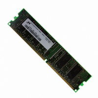
MT4VDDT3264AY-40BF1 Micron Technology Inc, MT4VDDT3264AY-40BF1 Datasheet - Page 10

MT4VDDT3264AY-40BF1
Manufacturer Part Number
MT4VDDT3264AY-40BF1
Description
MODULE DDR 256MB 184-UDIMM
Manufacturer
Micron Technology Inc
Datasheet
1.MT4VDDT3264AY-40BF1.pdf
(13 pages)
Specifications of MT4VDDT3264AY-40BF1
Memory Type
DDR SDRAM
Memory Size
256MB
Speed
200MHz
Package / Case
184-DIMM
Main Category
DRAM Module
Sub-category
DDR SDRAM
Module Type
184UDIMM
Device Core Size
64b
Organization
32Mx64
Total Density
256MByte
Chip Density
512Mb
Maximum Clock Rate
400MHz
Operating Supply Voltage (typ)
2.6V
Operating Current
860mA
Number Of Elements
4
Operating Supply Voltage (max)
2.7V
Operating Supply Voltage (min)
2.5V
Operating Temp Range
0C to 70C
Operating Temperature Classification
Commercial
Pin Count
184
Mounting
Socket
Lead Free Status / RoHS Status
Lead free / RoHS Compliant
Other names
557-1342
Table 10:
PDF: 09005aef8085081a/Source: 09005aef806e129d
DD4C16_32x64A.fm - Rev. E 11/08 EN
Parameter/Condition
Operating one device bank active-precharge current:
(MIN);
cycle; Address and control inputs changing once every two clock cycles
Operating one device bank active-read-precharge current:
Burst = 4;
control inputs changing once per clock cycle
Precharge power-down standby current: All device banks idle; Power-
down mode;
Idle standby current: CS# = HIGH; All device banks idle;
CKE = HIGH; Address and other control inputs changing once per clock
cycle; Vin = Vref for DQ, DQS, and DM
Active power-down standby current: One device bank active; Power-
down mode;
Active standby current: CS# = HIGH; CKE = HIGH; One device bank
active;
changing twice per clock cycle; Address and other control inputs changing
once per clock cycle
Operating burst read current: Burst = 2; Continuous burst reads; One
device bank active; Address and control inputs changing once per clock
cycle;
Operating burst write current: Burst = 2; Continuous burst writes; One
device bank active; Address and control inputs changing once per clock
cycle;
cycle
Auto refresh current
Self refresh current: CKE ≤ 0.2V
Operating bank interleave read current: Four device bank
interleaving READs (burst = 4) with auto precharge;
t
READ or WRITE commands
CK =
t
t
t
CK (MIN); Address and control inputs change only during active
t
CK =
CK =
t
CK =
RC =
t
RC =
t
t
t
CK (MIN); Iout = 0mA
CK (MIN); DQ, DM, and DQS inputs changing twice per clock
t
CK (MIN); DQ, DM, and DQS inputs changing once per clock
t
t
RAS (MAX);
Idd Specifications and Conditions – 128MB (All Other Die Revisions)
Values are for the MT46V16M16 DDR SDRAM only and are computed from values specified in the
256Mb (16 Meg x 16) component data sheet
CK =
CK =
t
RC (MIN);
t
t
CK (MIN); CKE = LOW
CK (MIN); CKE = LOW
t
t
CK =
CK =
t
t
CK (MIN); DQ, DM, and DQS inputs
CK (MIN); Iout = 0mA; Address and
128MB, 256MB (x64, SR) 184-Pin DDR SDRAM UDIMM
t
t
t
RC =
RFC =
RFC = 7.8125µs
t
CK =
t
RC (MIN);
t
10
t
RC =
RFC (MIN)
t
CK (MIN);
t
RC
Micron Technology, Inc., reserves the right to change products or specifications without notice.
Symbol
Idd4W
Idd3N
Idd5A
Idd2P
Idd3P
Idd4R
Idd2F
Idd0
Idd1
Idd5
Idd6
Idd7
-40B
1040
1040
2040
540
740
240
160
280
860
16
24
16
Electrical Specifications
1020
1760
-335
©2003 Micron Technology, Inc. All rights reserved.
500
720
200
120
240
880
780
16
24
16
1520
-262
500
680
180
100
200
740
640
940
16
24
16
-26A/
1520/
-265 Units
1600
100/
940/
480
620
180
120
200
740
640
980
16
24
16
mA
mA
mA
mA
mA
mA
mA
mA
mA
mA
mA
mA


