TLP181(GB,F,T) Toshiba, TLP181(GB,F,T) Datasheet - Page 3
TLP181(GB,F,T)
Manufacturer Part Number
TLP181(GB,F,T)
Description
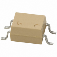
PHOTOCOUPLER TRANS-OUT 4-SMD
Manufacturer
Toshiba
Specifications of TLP181(GB,F,T)
Number Of Channels
1
Input Type
DC
Voltage - Isolation
3750Vrms
Current Transfer Ratio (min)
100% @ 5mA
Current Transfer Ratio (max)
600% @ 5mA
Voltage - Output
80V
Current - Output / Channel
50mA
Current - Dc Forward (if)
50mA
Vce Saturation (max)
400mV
Output Type
Transistor
Mounting Type
Surface Mount
Package / Case
4-SMD
Configuration
1 Channel
Maximum Collector Emitter Voltage
80 V
Maximum Collector Emitter Saturation Voltage
0.4 V
Isolation Voltage
3750 Vrms
Current Transfer Ratio
100 % to 600 %
Maximum Forward Diode Voltage
1.3 V
Minimum Forward Diode Voltage
1 V
Maximum Power Dissipation
200 mW
Maximum Operating Temperature
+ 100 C
Minimum Operating Temperature
- 55 C
Forward Current
10 mA
Maximum Input Diode Current
10 mA
Output Device
Phototransistor
Number Of Elements
1
Reverse Breakdown Voltage
5V
Forward Voltage
1.3V
Collector-emitter Voltage
80V
Package Type
MFSOP
Collector Current (dc) (max)
50mA
Power Dissipation
200mW
Collector-emitter Saturation Voltage
0.4V
Pin Count
4
Mounting
Surface Mount
Operating Temp Range
-25C to 85C
Operating Temperature Classification
Commercial
Lead Free Status / RoHS Status
Lead free / RoHS Compliant
Other names
TLP181GBF


Absolute Maximum Ratings
Recommended Operating Conditions
Storage temperature range
Operating temperature range
Lead soldering temperature
Total package power dissipation
Total package power dissipation
derating (Ta ≥ 25°C)
Isolation voltage
(AC, 1min., R.H. ≤ 60%)
Note: Using continuously under heavy loads (e.g. the application of high temperature/current/voltage and the
(Note 1) Device considered a two−terminal device: Pin1, 3 shorted together and pins 4, 6 shorted together
Supply voltage
Forward current
Collector current
Note: Recommended operating conditions are given as a design guideline to obtain expected performance of the
Forward current
Forward current detating
Pulse forward current
(100μs pulse, 100pps)
Reverse voltage
Junction temperature
Collector−emitter voltage
Emitter−collector voltage
Collector current
Collector power dissipation
(1 Circuit)
Collector power dissipation
derating (1 Circuit Ta ≥ 25°C)
Junction temperature
significant change in temperature, etc.) may cause this product to decrease in the reliability significantly even
if the operating conditions (i.e. operating temperature/current/voltage, etc.) are within the absolute maximum
ratings.
Please design the appropriate reliability upon reviewing the Toshiba Semiconductor Reliability Handbook
(“Handling Precautions”/“Derating Concept and Methods”) and individual reliability data (i.e. reliability test
report and estimated failure rate, etc).
device. Additionally, each item is an independent guideline respectively. In developing designs using this
product, please confirm specified characteristics shown in this document.
Characteristic
Characteristic
(Note 1)
(Ta = 25°C)
ΔP
ΔP
ΔI
Symbol
V
V
T
BV
T
T
F
I
V
P
CEO
ECO
C
P
T
I
I
FP
T
T
stg
opr
sol
C
F
/ °C
R
C
T
j
j
/ °C
/ °C
S
Symbol
V
I
I
CC
C
F
3
−1.4 (Ta ≥89°C)
Min
―
―
―
−55 to 125
−55 to 110
260 (10s)
Rating
3750
−1.5
−2.0
125
150
125
200
50
80
50
1
5
7
Typ.
16
5
1
Max
48
20
10
Unit
mA
mA
V
mW / °C
mW / °C
mA / °C
V
Unit
mW
mW
mA
mA
°C
°C
°C
°C
°C
rms
A
V
V
V
2009-11-12
TLP181
Related parts for TLP181(GB,F,T)
Image
Part Number
Description
Manufacturer
Datasheet
Request
R

Part Number:
Description:
PHOTOCOUPLER TRANS OUT 4-SMD
Manufacturer:
Toshiba
Datasheet:

Part Number:
Description:
PHOTOCOUPLER TRANS OUT 6MFSOP-4
Manufacturer:
Toshiba
Datasheet:
Part Number:
Description:
PHOTOCOUPLER TRANS-OUT 4-SMD
Manufacturer:
Toshiba
Datasheet:
Part Number:
Description:
Transistor Output Optocouplers 80Vceo 3750Vrms High CTR
Manufacturer:
Toshiba
Part Number:
Description:
IC OPTOCOUPL AC/DC-IN 1-CH TRANS DC-OUT 4MFSOP
Manufacturer:
Toshiba
Datasheet:
Part Number:
Description:
GaAs IRED & PHOTO-TRANSISTOR
Manufacturer:
Toshiba
Datasheet:
Part Number:
Description:
PHOTOCOUPLER TRANS-OUT 4-SMD
Manufacturer:
Toshiba
Datasheet:
Part Number:
Description:
PHOTOCOUPLER TRANS-OUT 4-SMD
Manufacturer:
Toshiba
Datasheet:
Part Number:
Description:
PHOTOCOUPLER TRANS OUT 4-SMD
Manufacturer:
Toshiba
Datasheet:
Part Number:
Description:
PHOTOCOUPLER TRANS OUT 4-SMD
Manufacturer:
Toshiba
Datasheet:
Part Number:
Description:
PHOTOCOUPLER TRANS OUT 4-SMD
Manufacturer:
Toshiba
Datasheet:
Part Number:
Description:
PHOTOCOUPLER TRANS OUT 4-SMD
Manufacturer:
Toshiba
Datasheet:
Part Number:
Description:
PHOTOCOUPLER TRANS OUT 4-SMD
Manufacturer:
Toshiba
Datasheet:
Part Number:
Description:
PHOTOCOUPLER TRANS OUT 4-SMD
Manufacturer:
Toshiba
Datasheet: