IL300-EF Vishay, IL300-EF Datasheet - Page 12
IL300-EF
Manufacturer Part Number
IL300-EF
Description
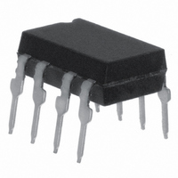
OPTOCOUPLER HI GAIN WIDE BW 8DIP
Manufacturer
Vishay
Specifications of IL300-EF
Isolation Voltage
5300 Vrms
Number Of Channels
2
Input Type
DC
Voltage - Isolation
5300Vrms
Current Transfer Ratio (min)
0.85% @ 10mA
Current Transfer Ratio (max)
1.06% @ 10mA
Current - Dc Forward (if)
60mA
Output Type
Linear Photovoltaic
Mounting Type
Through Hole
Package / Case
8-DIP (0.300", 7.62mm)
Current Transfer Ratio
0.5 % to 1.1 %
Forward Current
10 mA
Maximum Fall Time
1.75 us
Maximum Rise Time
1.75 us
Output Device
PIN Photodiode
Configuration
1 Channel
Maximum Forward Diode Voltage
1.5 V
Maximum Reverse Diode Voltage
5 V
Maximum Input Diode Current
60 mA
Maximum Power Dissipation
210 mW
Maximum Operating Temperature
+ 100 C
Minimum Operating Temperature
- 55 C
No. Of Channels
1
Optocoupler Output Type
Photodiode
Input Current
10mA
Output Voltage
50V
Opto Case Style
DIP
No. Of Pins
8
Gain Db Max
1.061dB
Lead Free Status / RoHS Status
Lead free / RoHS Compliant
Voltage - Output
-
Current - Output / Channel
-
Vce Saturation (max)
-
Lead Free Status / Rohs Status
Lead free / RoHS Compliant
Other names
751-1295-5
IL300-EFGI
IL300-EFGI
IL300-EFGI
IL300-EFGI
Available stocks
Company
Part Number
Manufacturer
Quantity
Price
Company:

Part Number:
IL300-EF-X007T
Manufacturer:
AD
Quantity:
246


IL300
Vishay Semiconductors
Table 2. Optolinear amplifiers
These amplifiers provide either an inverting or non-
inverting transfer gain based upon the type of input
and output amplifier. Table 2 shows the various con-
figurations along with the specific transfer gain equa-
tions. The offset column refers to the calculation of the
output offset or V
www.vishay.com
12
iil300_22
Vin
R1
R1
Vin
17189
Inverting
Non-Inverting
Non-Inverting Input
R2
R2
Inverting Input
–Vref1
+Vref1
3
2
3
2
+
+
R3
R3
–
–
4
4
Inverting
Non-Inverting Non-Inverting
Inverting
Non-Inverting
ref2
7
7
–Vcc
20pF
Vcc
Vcc
Vcc
necessary to provide a zero volt-
6
6
20pF
+Vcc
100
100
–Vcc
–Vcc
+Vcc
Inverting
Non-Inverting
Inverting
1
2
3
4
1
2
3
4
IL 300
IL 300
Figure 22. Non-inverting and Inverting Amplifiers
Non-Inverting Output
V OUT
V OUT
8
7
6
5
8
7
6
5
V IN
V OUT
V IN
V IN
V OUT
Inverting Output
V IN
Vcc
Vcc
+Vref2
=
=
=
=
R4
- K3 R4 R2 (R5 + R6)
K3 R4 R2 (R5 + R6)
2
3
3
2
+Vref2
R5
R3 (R1 + R2)
R3 R5 (R1 + R2)
R3 R5 (R1 + R2)
-
R3 (R1 + R2)
+
+
–
K3 R4 R2
–
K3 R4 R2
R4
R6
7
4
7
–Vcc
4
Vcc
Vcc
–Vcc
age output for a zero voltage input. The non-inverting
input amplifier requires the use of a bipolar supply,
while the inverting input stage can be implemented
with single supply operational amplifiers that permit
operation close to ground.
Vo
6
6
Vout
V ref2 =
V ref2 =
V ref2 =
V ref2 =
- V ref1
V ref1 R4 K3
- V ref1 R4 K3
V ref1
R3 R6
R3 R6
R3
R3
R4 (R5 + R6) K3
R4 (R5 + R6) K3
Document Number 83622
Rev. 1.5, 24-Mar-05
VISHAY
Related parts for IL300-EF
Image
Part Number
Description
Manufacturer
Datasheet
Request
R

Part Number:
Description:
OPTOCOUPLER HI GAIN WIDE BW 8DIP
Manufacturer:
Vishay
Datasheet:
Part Number:
Description:
OPTOCOUPLER HI GAIN WIDE BW 8DIP
Manufacturer:
Vishay
Datasheet:
Part Number:
Description:
OPTOCOUPLER HI GAIN WIDE BW 8DIP
Manufacturer:
Vishay
Datasheet:
Part Number:
Description:
OPTOCOUPLER HI GAIN WIDE BW 8DIP
Manufacturer:
Vishay
Datasheet:

Part Number:
Description:
High Linearity Optocouplers Single Linear, High Gain, Wide Bandwidth
Manufacturer:
Vishay
Part Number:
Description:
High Linearity Optocouplers Single Linear, High Gain, Wide Bandwidth
Manufacturer:
Vishay
Part Number:
Description:
High Linearity Optocouplers Single Linear, High Gain, Wide Bandwidth
Manufacturer:
Vishay

Part Number:
Description:
Linear Optocoupler, High Gain Stability, Wide Bandwidth
Manufacturer:
VISHAY [Vishay Siliconix]
Datasheet:

Part Number:
Description:
OPTOCOUPLER, PHOTODIODE, 5300VRMS
Manufacturer:
Vishay
Datasheet: