TCET1100 Vishay, TCET1100 Datasheet - Page 6
TCET1100
Manufacturer Part Number
TCET1100
Description
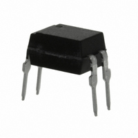
OPTOCOUPLER PHOTOTRANS 600% 4DIP
Manufacturer
Vishay
Specifications of TCET1100
Mounting Type
Through Hole
Isolation Voltage
5000 Vrms
Number Of Channels
1
Input Type
DC
Voltage - Isolation
5000Vrms
Current Transfer Ratio (min)
50% @ 5mA
Current Transfer Ratio (max)
600% @ 5mA
Voltage - Output
70V
Current - Output / Channel
50mA
Current - Dc Forward (if)
60mA
Vce Saturation (max)
300mV
Output Type
Transistor
Package / Case
4-DIP (0.300", 7.62mm)
Maximum Input Diode Current
60 mA
Maximum Reverse Diode Voltage
6 V
Output Device
Transistor
Configuration
1
Maximum Collector Emitter Voltage
70 V
Maximum Collector Emitter Saturation Voltage
300 mV
Current Transfer Ratio
600 %
Maximum Forward Diode Voltage
1.6 V
Maximum Collector Current
50 mA
Maximum Power Dissipation
265 mW
Maximum Operating Temperature
+ 100 C
Minimum Operating Temperature
- 40 C
No. Of Channels
1
Optocoupler Output Type
Phototransistor
Input Current
50mA
Output Voltage
70V
Opto Case Style
DIP
No. Of Pins
4
Approval Bodies
VDE, CSA, BSI EN
Rohs Compliant
Yes
Lead Free Status / RoHS Status
Lead free / RoHS Compliant
Lead Free Status / RoHS Status
Lead free / RoHS Compliant, Lead free / RoHS Compliant
Available stocks
Company
Part Number
Manufacturer
Quantity
Price

Part Number:
TCET1100G
Manufacturer:
VISHAY/威世
Quantity:
20 000


TCET1100/TCET1100G
Vishay Semiconductors
Switching Characteristics
www.vishay.com
6
Delay time
Rise time
Turn-on time
Storage time
Fall time
Turn-off time
Turn-on time
Turn-off time
95 10804
95 10843
0
R
t
T
p
t
G
p
0
R
t
= 0.01
T
= 5 0 µs
= 5 0 Ω
p
t
G
p
Figure 3. Test circuit, non-saturated operation
= 0.01
Parameter
= 50 µs
= 50
Figure 4. Test circuit, saturated operation
I
F
I
F
50
I
F
50
Ω
= 1 0 m A
I
F
1 k
100
Ω
V
(see figure 3)
V
(see figure 3)
V
(see figure 3)
V
(see figure 3)
V
(see figure 3)
V
(see figure 3)
V
(see figure 4)
V
(see figure 4)
+ 5 V
I
Channel II
S
S
S
S
S
S
S
S
Channel I
C
+ 5 V
= 5 V, I
= 5 V, I
= 5 V, I
= 5 V, I
= 5 V, I
= 5 V, I
= 5 V, I
= 5 V, I
I
Channel II
C
Channel I
= 2 mA; adjusted through
Test condition
C
C
C
C
C
C
F
F
= 2 mA, R
= 2 mA, R
= 2 mA, R
= 2 mA, R
= 2 mA, R
= 2 mA, R
= 10 mA, R
= 10 mA, R
input amplitude
R
C
Oscilloscope
Oscilloscope
R
C
L
L
L
L
≤
≥
= 1 M
= 20 pF
1
20 pF
L
L
L
L
L
L
M
L
L
= 100 Ω
= 100 Ω
= 100 Ω
= 100 Ω
= 100 Ω
= 100 Ω
Ω
= 1 kΩ
= 1 kΩ
Symbol
t
t
t
t
t
on
t
off
on
off
t
t
d
s
r
f
t
t
t
t
p
d
r
on
(=t + t )
100 %
10 %
90 %
d
I
I
C
r
F
0
0
Min
t
pulse duration
delay time
rise time
turn-on time
d
t
Figure 5. Switching Times
on
t
r
t
p
10.0
Typ.
3.0
3.0
6.0
0.3
4.7
5.0
9.0
t
t
t
t
s
f
off
s
(= t
Document Number 83503
s
t
off
+ t
t
f
Max
f
)
Rev. 2.2, 05-Sep-06
storage time
fall time
turn-off time
96 11698
t
t
Unit
µs
µs
µs
µs
µs
µs
µs
µs
Related parts for TCET1100
Image
Part Number
Description
Manufacturer
Datasheet
Request
R

Part Number:
Description:
357-036-542-201 CARDEDGE 36POS DL .156 BLK LOPRO
Manufacturer:
Vishay
Datasheet:
Part Number:
Description:
357-036-542-201 CARDEDGE 36POS DL .156 BLK LOPRO
Manufacturer:
Vishay
Datasheet:
Part Number:
Description:
357-036-542-201 CARDEDGE 36POS DL .156 BLK LOPRO
Manufacturer:
Vishay
Datasheet:
Part Number:
Description:
357-036-542-201 CARDEDGE 36POS DL .156 BLK LOPRO
Manufacturer:
Vishay
Datasheet:
Part Number:
Description:
357-036-542-201 CARDEDGE 36POS DL .156 BLK LOPRO
Manufacturer:
Vishay
Datasheet:
Part Number:
Description:
357-036-542-201 CARDEDGE 36POS DL .156 BLK LOPRO
Manufacturer:
Vishay
Datasheet:
Part Number:
Description:
357-036-542-201 CARDEDGE 36POS DL .156 BLK LOPRO
Manufacturer:
Vishay
Datasheet:
Part Number:
Description:
357-036-542-201 CARDEDGE 36POS DL .156 BLK LOPRO
Manufacturer:
Vishay
Datasheet:
Part Number:
Description:
357-036-542-201 CARDEDGE 36POS DL .156 BLK LOPRO
Manufacturer:
Vishay
Datasheet:
Part Number:
Description:
357-036-542-201 CARDEDGE 36POS DL .156 BLK LOPRO
Manufacturer:
Vishay
Datasheet:
Part Number:
Description:
357-036-542-201 CARDEDGE 36POS DL .156 BLK LOPRO
Manufacturer:
Vishay
Datasheet:
Part Number:
Description:
357-036-542-201 CARDEDGE 36POS DL .156 BLK LOPRO
Manufacturer:
Vishay
Datasheet:
Part Number:
Description:
357-036-542-201 CARDEDGE 36POS DL .156 BLK LOPRO
Manufacturer:
Vishay
Datasheet:
Part Number:
Description:
357-036-542-201 CARDEDGE 36POS DL .156 BLK LOPRO
Manufacturer:
Vishay
Datasheet:
Part Number:
Description:
357-036-542-201 CARDEDGE 36POS DL .156 BLK LOPRO
Manufacturer:
Vishay
Datasheet: