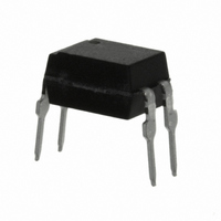
TCET1100 Vishay, TCET1100 Datasheet
TCET1100
Specifications of TCET1100
Available stocks


Related parts for TCET1100

TCET1100 Summary of contents
Page 1
... The elements are mounted on one leadframe using a coplanar technique, providing a fixed distance between input and output for highest safety require- ments. Isolation materials according to UL94-VO Document Number 83503 Rev. 2.2, 05-Sep-06 TCET1100/TCET1100G Vishay Semiconductors ...
Page 2
... CTR 50 - 150 %, DIP-4 TCET1106 CTR 100 - 300 %, DIP-4 TCET1107 CTR 80 - 160 %, DIP-4 TCET1108 CTR 130 - 260 %, DIP-4 TCET1109 CTR 200 - 400 %, DIP-4 TCET1100G CTR 50 - 600 %, DIP-4 TCET1101G CTR DIP-4 TCET1102G CTR 63 - 125 %, DIP-4 TCET1103G CTR 100 - 200 %, DIP-4 TCET1104G CTR 160 - 320 %, DIP-4 ...
Page 3
... Thermal resistance, Board to Ambient* Thermal resistance, Case to Ambient* * For 2 layer FR4 board (4" x 3" x 0.062 θ DC θ θ 19996 Document Number 83503 Rev. 2.2, 05-Sep-06 TCET1100/TCET1100G Test condition Symbol V ISO T amb T stg T sld Test condition at 25 ° °C θ CA Package θ θ ...
Page 4
... Test condition Symbol = CEsat = 10 mA Test condition Part TCET1101 = TCET1101G TCET1102 TCET1102G TCET1103 TCET1103G TCET1104 TCET1104G TCET1100 = TCET1100G TCET1105 TCET1105G TCET1106 TCET1106G TCET1107 TCET1107G TCET1108 TCET1108G TCET1109 TCET1109G TCET1101 = TCET1101G TCET1102 TCET1102G TCET1103 TCET1103G TCET1104 TCET1104G Min Typ. Max 1.25 1.6 50 Min Typ ...
Page 5
... Phototransistor 250 Psi (mW) 200 150 100 IR-Diode 50 Isi (mA 100 T - Safety Temperature (°C) 94 9182 si Figure 1. Derating diagram Document Number 83503 Rev. 2.2, 05-Sep-06 TCET1100/TCET1100G Test condition Symbol I F Test condition Symbol P diss Test condition Symbol V IOTM T si Test condition Symbol = test ...
Page 6
... TCET1100/TCET1100G Vishay Semiconductors Switching Characteristics Parameter Delay time (see figure 3) Rise time (see figure 3) Turn-on time (see figure 3) Storage time (see figure 3) Fall time (see figure 3) Turn-off time (see figure 3) Turn-on time (see figure 4) Turn-off time (see figure mA; adjusted through 0.01 ...
Page 7
... T - Ambient Temperature (°C) amb Figure 8. Relative Current Transfer Ratio vs. Ambient Temperature Document Number 83503 Rev. 2.2, 05-Sep-06 TCET1100/TCET1100G 10000 1000 100 120 95 11026 Figure 9. Collector Dark Current vs. Ambient Temperature 100 0.1 0.01 2.0 1.4 1.6 1.8 95 11027 Figure 10. Collector Current vs. Forward Current ...
Page 8
... TCET1100/TCET1100G Vishay Semiconductors 1 0.8 CTR = 50 % 0.6 0.4 0 Collector Current (mA) 95 11028 C Figure 12. Collector Emitter Saturation Voltage vs. Collector Current 1000 100 Forward Current (mA) 95 11029 F Figure 13. Current Transfer Ratio vs. Forward Current 10 Non Saturated Operation 100 Ω off Collector Current (mA) 95 11030 C Figure 14 ...
Page 9
... Package Dimensions in mm Package Dimensions in mm Document Number 83503 Rev. 2.2, 05-Sep-06 TCET1100/TCET1100G Vishay Semiconductors 14789 14792 www.vishay.com 9 ...
Page 10
... TCET1100/TCET1100G Vishay Semiconductors Ozone Depleting Substances Policy Statement It is the policy of Vishay Semiconductor GmbH to 1. Meet all present and future national and international statutory requirements. 2. Regularly and continuously improve the performance of our products, processes, distribution and operating systems with respect to their impact on the health and safety of our employees and the public, as well as their impact on the environment ...
Page 11
... Information contained herein is intended to provide a product description only. No license, express or implied, by estoppel or otherwise, to any intellectual property rights is granted by this document. Except as provided in Vishay's terms and conditions of sale for such products, Vishay assumes no liability whatsoever, and disclaims any express or implied warranty, relating to sale and/or use of Vishay products including liability or warranties relating to fitness for a particular purpose, merchantability, or infringement of any patent, copyright, or other intellectual property right ...