TCET1103 Vishay, TCET1103 Datasheet - Page 5
TCET1103
Manufacturer Part Number
TCET1103
Description
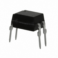
OPTOCOUPLER PHOTOTRANS 200% 4DIP
Manufacturer
Vishay
Specifications of TCET1103
Mounting Type
Through Hole
Isolation Voltage
5000 Vrms
Number Of Channels
1
Input Type
DC
Voltage - Isolation
5000Vrms
Current Transfer Ratio (min)
34% @ 1mA
Current Transfer Ratio (max)
200% @ 10mA
Voltage - Output
70V
Current - Output / Channel
50mA
Current - Dc Forward (if)
60mA
Vce Saturation (max)
300mV
Output Type
Transistor
Package / Case
4-DIP (0.300", 7.62mm)
Forward Current
60 mA
Maximum Input Diode Current
60 mA
Maximum Reverse Diode Voltage
6 V
Output Device
Transistor
Configuration
1
Maximum Collector Emitter Voltage
70 V
Maximum Collector Emitter Saturation Voltage
300 mV
Current Transfer Ratio
200 %
Maximum Forward Diode Voltage
1.6 V
Maximum Collector Current
50 mA
Maximum Power Dissipation
265 mW
Maximum Operating Temperature
+ 100 C
Minimum Operating Temperature
- 40 C
No. Of Channels
1
Optocoupler Output Type
Phototransistor
Input Current
50mA
Output Voltage
70V
Opto Case Style
DIP
No. Of Pins
4
Approval Bodies
VDE, CSA, BSI EN
Rohs Compliant
Yes
Lead Free Status / RoHS Status
Lead free / RoHS Compliant
Lead Free Status / RoHS Status
Lead free / RoHS Compliant, Lead free / RoHS Compliant
Available stocks
Company
Part Number
Manufacturer
Quantity
Price
Company:

Part Number:
TCET1103
Manufacturer:
Telefunk
Quantity:
15 045
Company:
Part Number:
TCET1103
Manufacturer:
FUJ
Quantity:
2 000
Part Number:
TCET1103
Manufacturer:
VISHAY/威世
Quantity:
20 000
Part Number:
TCET1103G
Manufacturer:
VISHAY/威世
Quantity:
20 000


Maximum Safety Ratings
(according to DIN EN 60747-5-2(VDE0884)/ DIN EN 60747-5-5 pending) see figure 1.
Input
Output
Coupler
Insulation Rated Parameters
Document Number 83503
Rev. 2.2, 05-Sep-06
This optocoupler is suitable for safe electrical isolation only within the safety ratings.
Compliance with the safety ratings shall be ensured by means of suitable protective circuits.
Forward current
Power dissipation
Rated impulse voltage
Safety temperature
Partial discharge test voltage -
Routine test
Partial discharge test voltage -
Lot test (sample test)
Insulation resistance
94 9182
Parameter
Parameter
Parameter
Parameter
300
250
200
150
100
50
0
0
Figure 1. Derating diagram
25
T
si
- Safety Temperature (°C)
IR-Diode
Isi (mA)
50
Phototransistor
Psi (mW)
75
100 %, t
t
(see figure 2)
V
V
V
(construction test only)
Tr
IO
IO
IO
= 60 s, t
= 500 V
= 500 V, T
= 500 V, T
100
test
Test condition
Test condition
Test condition
Test condition
test
125
= 1 s
= 10 s,
amb
amb
150
= 100 °C
= 150 °C
Figure 2. Test pulse diagram for sample test according to DIN EN
Symbol
Symbol
Symbol
Symbol
V
V
P
V
V
R
R
R
IOTM
T
IOTM
I
diss
F
pd
pd
IO
IO
IO
si
TCET1100/TCET1100G
13930
V
V
V
IOWM
IOTM
IORM
60747-5-2(VDE0884)/ DIN EN 60747-; IEC60747
V
Pd
0
t
1
10
10
Min
Min
Min
Min
10
1.6
1.3
8
12
11
9
t
t
t
1
3
stres
t
test
, t
, t
2
4
t
Tr
Vishay Semiconductors
= 1 to 10 s
= 1 s
= 10 s
= 12 s
Typ.
Typ.
Typ.
Typ.
= 60 s
Max
Max
Max
Max
130
265
150
8
t
2
t
3
www.vishay.com
t
t
stres
test
t
t
4
Unit
Unit
mW
Unit
Unit
mA
kV
°C
kV
kV
kV
Ω
Ω
Ω
5
Related parts for TCET1103
Image
Part Number
Description
Manufacturer
Datasheet
Request
R

Part Number:
Description:
357-036-542-201 CARDEDGE 36POS DL .156 BLK LOPRO
Manufacturer:
Vishay
Datasheet:
Part Number:
Description:
357-036-542-201 CARDEDGE 36POS DL .156 BLK LOPRO
Manufacturer:
Vishay
Datasheet:
Part Number:
Description:
357-036-542-201 CARDEDGE 36POS DL .156 BLK LOPRO
Manufacturer:
Vishay
Datasheet:
Part Number:
Description:
357-036-542-201 CARDEDGE 36POS DL .156 BLK LOPRO
Manufacturer:
Vishay
Datasheet:
Part Number:
Description:
357-036-542-201 CARDEDGE 36POS DL .156 BLK LOPRO
Manufacturer:
Vishay
Datasheet:
Part Number:
Description:
357-036-542-201 CARDEDGE 36POS DL .156 BLK LOPRO
Manufacturer:
Vishay
Datasheet:
Part Number:
Description:
357-036-542-201 CARDEDGE 36POS DL .156 BLK LOPRO
Manufacturer:
Vishay
Datasheet:
Part Number:
Description:
357-036-542-201 CARDEDGE 36POS DL .156 BLK LOPRO
Manufacturer:
Vishay
Datasheet:
Part Number:
Description:
357-036-542-201 CARDEDGE 36POS DL .156 BLK LOPRO
Manufacturer:
Vishay
Datasheet:
Part Number:
Description:
357-036-542-201 CARDEDGE 36POS DL .156 BLK LOPRO
Manufacturer:
Vishay
Datasheet:
Part Number:
Description:
357-036-542-201 CARDEDGE 36POS DL .156 BLK LOPRO
Manufacturer:
Vishay
Datasheet:
Part Number:
Description:
357-036-542-201 CARDEDGE 36POS DL .156 BLK LOPRO
Manufacturer:
Vishay
Datasheet:
Part Number:
Description:
357-036-542-201 CARDEDGE 36POS DL .156 BLK LOPRO
Manufacturer:
Vishay
Datasheet:
Part Number:
Description:
357-036-542-201 CARDEDGE 36POS DL .156 BLK LOPRO
Manufacturer:
Vishay
Datasheet:
Part Number:
Description:
357-036-542-201 CARDEDGE 36POS DL .156 BLK LOPRO
Manufacturer:
Vishay
Datasheet: