6N139(F) Toshiba, 6N139(F) Datasheet - Page 4
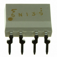
6N139(F)
Manufacturer Part Number
6N139(F)
Description
PHOTOCOUPLER HS DARL-OUT 8-DIP
Manufacturer
Toshiba
Datasheet
1.6N139F.pdf
(6 pages)
Specifications of 6N139(F)
Voltage - Isolation
2500Vrms
Number Of Channels
1, Unidirectional
Current - Output / Channel
60mA
Propagation Delay High - Low @ If
5µs @ 500µA
Current - Dc Forward (if)
20mA
Input Type
DC
Output Type
Logic
Mounting Type
Through Hole
Package / Case
8-DIP (0.300", 7.62mm)
Voltage - Output
18V
Current Transfer Ratio (min)
400% @ 500µA
Configuration
1 Channel
Current Transfer Ratio
900 %
Maximum Baud Rate
100 KBps
Maximum Forward Diode Voltage
1.7 V
Maximum Reverse Diode Voltage
5 V
Maximum Input Diode Current
20 mA
Maximum Power Dissipation
100 mW
Maximum Operating Temperature
+ 70 C
Minimum Operating Temperature
0 C
Isolation Voltage
2500 Vrms
Maximum Fall Time
25 us
Maximum Rise Time
60 us
Output Device
Photodarlington
Lead Free Status / RoHS Status
Lead free / RoHS Compliant
Vce Saturation (max)
-
Current Transfer Ratio (max)
-
Lead Free Status / Rohs Status
Lead free / RoHS Compliant
Other names
6N139TF


Switching Specifications
Propagation delay
time to logic low
at output
Propagation delay
time to logic high
at output
Common mode transient
immunity at logic high
level output
Common mode transient
immunity at logic low
level output
(*)JEDEC registered data.
(Note 1): Derate linearly above 50°C free−air temperature at a rate of 0.4mA / °C
(Note 2): Derate linearly above 50°C free−air temperature at a rate of 0.7mW / °C
(Note 3): Derate linearly above 25°C free−air temperature at a rate of 0.7mA / °C
(Note 4): Derate linearly above 25°C free−air temperature at a rate of 2.0mW / °C
(Note 5): DC CURRENT TRANSFER RATIO is defined as the ratio of output collector current, I
(Note 6): Pin 7 open.
(Note 7): Device considered a two−terminal device: Pins 1, 2, 3, and 4 shorted together and Pins 5, 6, 7 and 8
(Note 8): Use of a resistor between pin 5 and 7 will decrease gain and delay time.
(Note 9): Common mode transient immunity in logic high level is the maximum tolerable (positive) dv
Characteristic
(Note 6, 8)
(Note 6, 8)
LED input current, I
shorted together.
the leading edge of the common mode pulse, V
state (i.e., V
Common mode transient immunity in Logic Low level is the maximum tolerable (negative) dv
the trailing edge of the common mode pulse signal, V
low state (i.e., V
(Note 9)
(Note 9)
6N139
6N138
6N139
6N138
O
> 2.0V).
O
< 0.8V).
(Ta=25°C, V
F
Symbol
t
t
pHL
pLH
, times 100%.
CM
CM
(*)
(*)
H
L
Test
Circuit
1
1
2
2
CC
=5V, unless otherwise specified)
I
I
I
I
I
I
I
V
I
R
V
F
F
F
F
F
F
F
F
CM
L
CM
=0.5mA, R
=12mA, R
=1.6mA, R
=0.5mA, R
=12mA, R
=1.6mA, R
=0mA, R
=1.6mA
=2.2kΩ
4
=400V
=400V
CM
Test Condition
L
p−p
p−p
=2.2kΩ
L
L
, to assure that the output will remain in a logic high
L
L
L
L
=270Ω
=270Ω
=4.7kΩ
=2.2kΩ
=4.7kΩ
=2.2kΩ
CM
, to assure that the output will remain in a logic
Min.
⎯
⎯
⎯
⎯
⎯
⎯
⎯
⎯
−500
Typ.
500
0.2
5
1
5
1
4
6N138,6N139
O
Max.
, to the forward
25
10
60
35
⎯
⎯
1
7
2007-10-01
CM
CM
V / μs
V / μs
/ dt on
Unit
μs
μs
/ dt on
Related parts for 6N139(F)
Image
Part Number
Description
Manufacturer
Datasheet
Request
R

Part Number:
Description:
PHOTOCOUPLER HS DARL-OUT 8-DIP
Manufacturer:
Toshiba
Datasheet:

Part Number:
Description:
High Speed Optocouplers IC CPLR, 300KBPS CTR 400%MIN Opto
Manufacturer:
Toshiba
Datasheet:

Part Number:
Description:
Toshiba Semiconductor [TOSHIBA IGBT Module Silicon N Channel IGBT]
Manufacturer:
TOSHIBA Semiconductor CORPORATION
Datasheet:
Part Number:
Description:
TOSHIBA GTR MODULE SILICON NPN TRIPLE DIFFUSED TYPE
Manufacturer:
TOSHIBA Semiconductor CORPORATION
Datasheet:
Part Number:
Description:
TOSHIBA GTR Module Silicon N Channel IGBT
Manufacturer:
TOSHIBA Semiconductor CORPORATION
Datasheet:
Part Number:
Description:
TOSHIBA Intelligent Power Module Silicon N Channel IGBT
Manufacturer:
TOSHIBA Semiconductor CORPORATION
Datasheet:
Part Number:
Description:
TOSHIBA INTELLIGENT POWER MODULE SILICON N CHANNEL LGBT
Manufacturer:
TOSHIBA Semiconductor CORPORATION
Datasheet:
Part Number:
Description:
TOSHIBA IGBT Module Silicon N Channel IGBT
Manufacturer:
TOSHIBA Semiconductor CORPORATION
Datasheet:
Part Number:
Description:
TOSHIBA GTR MODULE SILICON N−CHANNEL IGBT
Manufacturer:
TOSHIBA Semiconductor CORPORATION
Datasheet:
Part Number:
Description:
TOSHIBA Intelligent Power Module Silicon N Channel IGBT
Manufacturer:
TOSHIBA Semiconductor CORPORATION
Datasheet:
Part Number:
Description:
TOSHIBA GTR Module Silicon N Channel IGBT
Manufacturer:
TOSHIBA Semiconductor CORPORATION
Datasheet:
Part Number:
Description:
TOSHIBA INTELLIGENT POWER MODULE
Manufacturer:
TOSHIBA Semiconductor CORPORATION
Datasheet:
Part Number:
Description:
TOSHIBA Intelligent Power Module Silicon N Channel IGBT
Manufacturer:
TOSHIBA Semiconductor CORPORATION
Datasheet:
Part Number:
Description:
TOSHIBA Intelligent Power Module Silicon N Channel IGBT
Manufacturer:
TOSHIBA Semiconductor CORPORATION
Datasheet:
Part Number:
Description:
TOSHIBA IGBT Module Silicon N Channel IGBT
Manufacturer:
TOSHIBA Semiconductor CORPORATION
Datasheet: