TLP620(F,T) Toshiba, TLP620(F,T) Datasheet - Page 3
TLP620(F,T)
Manufacturer Part Number
TLP620(F,T)
Description
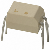
PHOTOCPLR AC IN TRANS-OUT 4-DIP
Manufacturer
Toshiba
Specifications of TLP620(F,T)
Number Of Channels
1
Input Type
AC, DC
Voltage - Isolation
5000Vrms
Current Transfer Ratio (min)
50% @ ±5mA
Current Transfer Ratio (max)
600% @ ±5mA
Voltage - Output
55V
Current - Output / Channel
50mA
Current - Dc Forward (if)
60mA
Vce Saturation (max)
400mV
Output Type
Transistor
Mounting Type
Through Hole
Package / Case
4-DIP (0.300", 7.62mm)
Output Device
Transistor
Number Of Elements
1
Forward Voltage
1.3V
Forward Current
60mA
Collector-emitter Voltage
55V
Package Type
PDIP
Collector Current (dc) (max)
50mA
Isolation Voltage
5000Vrms
Power Dissipation
250mW
Current Transfer Ratio
600%
Pin Count
4
Mounting
Through Hole
Operating Temp Range
-25C to 85C
Operating Temperature Classification
Commercial
Maximum Collector Emitter Voltage
55 V
Maximum Collector Emitter Saturation Voltage
0.4 V
Maximum Forward Diode Voltage
1.3 V
Maximum Collector Current
50 mA
Maximum Power Dissipation
250 mW
Maximum Operating Temperature
+ 100 C
Minimum Operating Temperature
- 55 C
Maximum Fall Time
3 us
Maximum Input Diode Current
60 mA
Maximum Rise Time
2 us
Lead Free Status / RoHS Status
Lead free / RoHS Compliant
Other names
TLP620F


Recommended Operating Conditions
Individual Electrical Characteristics
Coupled Electrical Characteristics
Supply voltage
Forward current
Collector current
Operating temperature
Note: Recommended operating conditions are given as a design guideline to obtain expected performance of the
Current transfer ratio
Saturated CTR
Collector−emitter saturation
voltage
Off−state collector current
CTR symmetry
Forward voltage
Forward current
Capacitance
Collector−emitter
breakdown voltage
Emitter−collector
breakdown voltage
Collector dark current
Capacitance
(collector to emitter)
device. Additionally, each item is an independent guideline respectively. In developing designs using this
product, please confirm specified characteristics shown in this document.
Characteristic
Characteristic
Characteristic
V
V
I
C
V
I
Symbol
Symbol
(BR) CEO
(BR) ECO
C (ratio)
I
I
CE (sat)
I
/ I
C (off)
C
C
CEO
V
C
I
CE
F (sat)
F
/ I
F
T
(Ta = 25°C)
I
F
Symbol
F (RMS)
(Ta = 25°C)
V
T
IC
opr
CC
I
V
V = 0, f = 1MHz
I
I
V
V
V
I
Rank GB
IF = ±1mA, V
Rank GB
I
I
Rank GB
V
I
F
C
E
F
C
C
C
F
CE
CE
CE
F
= ±10mA
= ±5mA, V
= 0.1mA
= 0.5mA
= 2.4mA, I
= 0.2 mA, I
(I
= ±0.7V
= ± 0.7V, V
3
F
= 24V
= 24V, Ta = 85°C
= 0, f = 1MHz
= −5mA) / I
Min.
−25
―
―
―
Test Condition
Test Condition
CE
F
CE
F
CE
= ±8mA
= ±1 mA
Typ.
= 5V
= 0.4V
16
―
C
5
1
= 24V
(I
TLP620,TLP620−2,TLP620−4
F
= +5mA)
Max.
24
20
10
85
Unit
mA
mA
°C
V
MIn.
0.33
Min.
100
1.0
55
50
30
―
―
―
―
―
―
―
―
―
―
7
Typ.
1.15
Typ.
2.5
0.2
60
10
10
60
―
―
―
―
―
―
―
2
1
1
2007-10-01
Max.
Max.
100
600
600
1.3
0.4
0.4
20
50
10
―
―
―
―
―
―
―
3
Unit
Unit
μA
μA
μA
pF
nA
pF
―
%
%
V
V
V
V
Related parts for TLP620(F,T)
Image
Part Number
Description
Manufacturer
Datasheet
Request
R

Part Number:
Description:
PHOTOCPLR DL AC IN TRANSOUT 8DIP
Manufacturer:
Toshiba
Datasheet:

Part Number:
Description:
Manufacturer:
TOSHIBA Semiconductor CORPORATION
Datasheet:

Part Number:
Description:
PHOTOCPLR QD AC IN TRANOUT 16DIP
Manufacturer:
Toshiba
Datasheet: