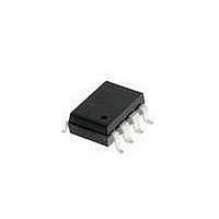
HCPL-2611-300E Avago Technologies US Inc., HCPL-2611-300E Datasheet - Page 10

HCPL-2611-300E
Manufacturer Part Number
HCPL-2611-300E
Description
OPTOCOUPLER 1CH 10MBD 8-SMD GW
Manufacturer
Avago Technologies US Inc.
Datasheet
1.HCPL-0600-500E.pdf
(22 pages)
Specifications of HCPL-2611-300E
Isolation Voltage
3750 Vrms
Maximum Fall Time
0.01 us
Minimum Forward Diode Voltage
1.4 V
Output Device
Logic Gate Photo IC
Configuration
1 Channel
Maximum Baud Rate
10 MBps
Maximum Forward Diode Voltage
1.75 V
Maximum Reverse Diode Voltage
5 V
Maximum Power Dissipation
85 mW
Maximum Operating Temperature
+ 85 C
Minimum Operating Temperature
- 40 C
Package / Case
DIP-8 Gull Wing
No. Of Channels
1
Optocoupler Output Type
Logic Gate
Input Current
15mA
Output Voltage
7V
Opto Case Style
SMD
No. Of Pins
8
Common Mode Ratio
10000
Rohs Compliant
Yes
Lead Free Status / RoHS Status
Lead free / RoHS Compliant
Lead Free Status / RoHS Status
Lead free / RoHS Compliant, Lead free / RoHS Compliant
Available stocks
Company
Part Number
Manufacturer
Quantity
Price
Company:
Part Number:
HCPL-2611-300E
Manufacturer:
AVAGO
Quantity:
10 000
Part Number:
HCPL-2611-300E
Manufacturer:
AVAGO/安华高
Quantity:
20 000
IEC/EN/DIN EN 60747-5-2 Insulation Related Characteristics
(HCPL-26xx; 46xx; 6N13x Option 060 Only)
*Refer to the front of the optocoupler section of the current catalog, under Product Safety Regulations section, IEC/EN/DIN EN 60747-5-2, for a
detailed description.
Note: Isolation characteristics are guaranteed only within the safety maximum ratings which must be ensured by protective circuits in applica-
tion.
IEC/EN/DIN EN 60747-5-2 Insulation Related Characteristics (HCNW137/2601/2611 Only)
*Refer to the front of the optocoupler section of the current catalog, under Product Safety Regulations section, IEC/EN/DIN EN 60747-5-2, for a
detailed description.
Note: Isolation characteristics are guaranteed only within the safety maximum ratings which must be ensured by protective circuits in applica-
tion.
10
Description
Installation classification per DIN VDE 0110/1.89, Table 1
Climatic Classification
Pollution Degree (DIN VDE 0110/1.89)
Maximum Working Insulation Voltage
Input to Output Test Voltage, Method b*
Input to Output Test Voltage, Method a*
Highest Allowable Overvoltage*
(Transient Overvoltage, t
Safety Limiting Values
Insulation Resistance at T
Description
Installation classification per DIN VDE 0110/1.89, Table 1
Climatic Classification (DIN IEC 68 part 1)
Pollution Degree (DIN VDE 0110/1.89)
Maximum Working Insulation Voltage
Input to Output Test Voltage, Method b*
Input to Output Test Voltage, Method a*
Highest Allowable Overvoltage*
(Transient Overvoltage, t
Safety Limiting Values
Insulation Resistance at T
V
V
V
V
for rated mains voltage ≤ 300 V rms
for rated mains voltage ≤ 450 V rms
Partial Discharge < 5 pC
t
(Maximum values allowed in the event of a failure,
also see Figure 16, Thermal Derating curve.)
for rated mains voltage ≤600 V rms
for rated mains voltage ≤1000 V rms
Partial Discharge < 5 pC
t
(Maximum values allowed in the event of a failure,
also see Figure 16, Thermal Derating curve.)
m
m
IORM
IORM
IORM
IORM
Case Temperature
Input Current
Output Power
Case Temperature
Input Current
Output Power
= 60 sec, Partial Discharge < 5 pC
= 60 sec, Partial Discharge < 5 pC
x 1.875 = V
x 1.5 = V
x 1.875 = V
x 1.5 = V
PR
PR
, Type and sample test,
, Type and sample test,
PR
PR
, 100% Production Test with t
, 100% Production Test with t
ini
ini
S
S
, V
, V
= 10 sec)
= 10 sec)
IO
IO
= 500 V
= 500 V
m
m
= 1 sec,
= 1 sec,
P
P
Symbol
Symbol
I
I
S,OUTPUT
S,OUTPUT
V
V
V
V
S,INPUT
S,INPUT
V
V
V
V
IORM
T
R
IORM
T
R
IOTM
IOTM
PR
PR
PR
PR
S
S
S
S
Characteristic
Characteristic
55/100/21
55/85/21
1181
6000
1414
2651
2121
8000
≥10
≥10
630
945
175
230
600
150
400
700
I-IV
I-III
I-IV
I-III
2
2
9
9
Units
Units
V
V
V
V
V
V
V
V
mW
mW
mA
mA
°C
°C
:
:
peak
peak
peak
peak
peak
peak
peak
peak


