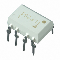
TLP251(F) Toshiba, TLP251(F) Datasheet - Page 2

TLP251(F)
Manufacturer Part Number
TLP251(F)
Description
PHOTOCOUPLER HS TRANS OUT 8-DIP
Manufacturer
Toshiba
Specifications of TLP251(F)
Voltage - Isolation
2500Vrms
Number Of Channels
1, Unidirectional
Current - Output / Channel
200mA
Propagation Delay High - Low @ If
250ns @ 8mA
Current - Dc Forward (if)
20mA
Input Type
DC
Output Type
Push-Pull, Totem-Pole
Mounting Type
Through Hole
Package / Case
8-DIP (0.300", 7.62mm)
Configuration
1 Channel
Maximum Forward Diode Voltage
1.8 V
Maximum Reverse Diode Voltage
5 V
Maximum Input Diode Current
20 mA
Maximum Operating Temperature
+ 85 C
Minimum Operating Temperature
- 20 C
Isolation Voltage
2500 Vrms
Maximum Fall Time
1 us
Maximum Rise Time
1 us
Output Device
Photo IC
Lead Free Status / RoHS Status
Lead free / RoHS Compliant
Other names
TLP251F
Absolute Maximum Ratings
Operating frequency
Operating temperature range
Storage temperature range
Lead soldering temperature(10s)
Isolation voltage (AC, 1min.,
R.H.≤ 60%)
Note: Using continuously under heavy loads (e.g. the application of high temperature/current/voltage and the
Note 1:
Note 2:
Note 3:
Note 4:
Note 5:
Forward current
Forward current derating
Peak transient forward current
Reverse voltage
Junction temperature
“
(P
“
(P
Output voltage
Supply voltage
Output voltage derating
(Ta ≥ 70°C)
Supply voltage derating
(Ta ≥ 70°C)
Junction temperature
H
L
significant change in temperature, etc.) may cause this product to decrease in the reliability significantly even
if the operating conditions (i.e. operating temperature/current/voltage, etc.) are within the absolute maximum
ratings.
Please design the appropriate reliability upon reviewing the Toshiba Semiconductor Reliability Handbook
(“Handling Precautions”/“Derating Concept and Methods”) and individual reliability data (i.e. reliability test
report and estimated failure rate, etc).
W
”
W
”
peak output current
peak output current
Pulse width P
Expornential waveform
Expornential waveform, I
Device considerd a two terminal device: Pins 1, 2, 3 and 4 shorted together, and pins 5, 6,
7 and 8 shorted together.
A ceramic capacitor(0.1μF)should be connected from pin 8 to pin 5 to stabilize the
operation of the high gain linear ampifier. Failure to provide the bypassing may impair the
swiching property.The total lead length between capacitor and coupler should not
exceed 1cm.
≤ 2.0μs, f ≤ 15kHz)
≤ 2.0μs, f ≤ 15kHz)
Characteristic
W
≤ 1μs, 300pps
OPH
≤ −0.25A(≤ 2.0μs), I
(Ta = 25°C)
(Ta ≤ 70°C)
(Ta = 85°C)
(Ta ≤ 70°C)
(Ta = 85°C)
(Ta ≥ 70°C)
(Note 1)
(Note 2)
(Note 2)
(Note 3)
(Note 4)
ΔV
ΔV
OPL
ΔI
Symbol
CC
F
I
I
O
I
V
T
BV
T
T
OPH
OPL
2
FPT
V
V
I
T
T
/ ΔTa
CC
opr
stg
sol
≤ +0.25A(≤2.0μs)
F
f
O
/ ΔTa
R
j
j
/ ΔTa
S
−55~125
−20~85
Rating
− 0.36
− 0.73
− 0.73
− 0.4
2500
125
125
260
0.4
20
35
24
35
24
25
1
5
mA / °C
V / °C
V / °C
Vrms
Unit
kHz
mA
°C
°C
°C
°C
°C
A
V
A
A
V
V
2007-10-01
TLP251


