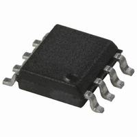
ACSL-6210-00RE Avago Technologies US Inc., ACSL-6210-00RE Datasheet - Page 17

ACSL-6210-00RE
Manufacturer Part Number
ACSL-6210-00RE
Description
OPTOCOUPLER DUAL BI 15MBD 8-SOIC
Manufacturer
Avago Technologies US Inc.
Datasheet
1.ACSL-6210-00RE.pdf
(19 pages)
Specifications of ACSL-6210-00RE
Package / Case
8-SOIC (0.154", 3.90mm Width)
Voltage - Isolation
2500Vrms
Number Of Channels
2, Bi-Directional
Current - Output / Channel
50mA
Data Rate
15MBd
Propagation Delay High - Low @ If
44ns @ 8mA
Current - Dc Forward (if)
15mA
Input Type
DC
Output Type
Open Collector
Mounting Type
Surface Mount
Isolation Voltage
2500 Vrms
Maximum Continuous Output Current
50 mA
Maximum Fall Time
0.012 us
Maximum Forward Diode Current
15 mA
Minimum Forward Diode Voltage
1.25 V
Output Device
Logic Gate Photo IC
Configuration
2 Channel
Maximum Baud Rate
15 MBd(Typ)
Maximum Forward Diode Voltage
1.8 V
Maximum Reverse Diode Voltage
5 V
Maximum Power Dissipation
60 mW
Maximum Operating Temperature
+ 100 C
Minimum Operating Temperature
- 40 C
No. Of Channels
2
Optocoupler Output Type
Logic Gate
Input Current
15mA
Output Voltage
7V
Opto Case Style
SOIC
No. Of Pins
8
Channel Type
Bi-directional
Rohs Compliant
Yes
Lead Free Status / RoHS Status
Lead free / RoHS Compliant
Lead Free Status / RoHS Status
Lead free / RoHS Compliant, Lead free / RoHS Compliant
Other names
516-1602-5
Available stocks
Company
Part Number
Manufacturer
Quantity
Price
Part Number:
ACSL-6210-00RE
Manufacturer:
AVAGO/安华高
Quantity:
20 000
With a CMOS gate to drive the optocoupler, the circuit
shown in Figure 19 can be used. The diode in parallel to
the current limiting resistor speeds the turn-off of the
optocoupler LED. Any HC or HCT series CMOS gate can
be used in this circuit.
For high common-mode rejection applications, the drive
circuit shown in Figure 20 is recommended. In this circuit,
only an open-collector TTL, or an open drain CMOS gate
can be used. This circuit drives the optocoupler LED with
a 220 ohm current-limiting resistor to ensure that an I
of 7 mA is applied under worst case conditions and thus
guarantee the 10,000 V/μs optocoupler common mode
rejection rating. The designer can obtain even higher
common-mode rejection performance than 10,000 V/μs
by driving the LED harder than 7 mA.
Phase Relationship to Input
The output of the optocoupler is inverted when
compared to the input. The input is defined to be logic
HIGH when the LED is ON. If there is a design that requires
the optocoupler to behave as a non-inverting gate, then
Figure 19. CMOS drive circuit for the ACSL-6xx0.
Figure 20. High CMR drive circuit for the ACSL-6xx0.
17
F
the series input drive circuit shown in Figure 19 can be
used. This input drive circuit has an inverting function,
and since the optocoupler also behaves as an inverter,
the total circuit is non-inverting. The shunt drive circuits
shown in Figures 18 and 20 will cause the optocoupler to
function as an inverter.
Current and Voltage Limitations
The absolute maximum voltage allowable at the output
supply voltage pin and the output voltage pin of the opt-
ocoupler is 7 volts. However, the recommended maximum
voltage at these two pins is 5.5 volts. The output sinking
current should not exceed 13 mA in order to make the
Low Level Output Voltage be less than 0.6 volt. If the
output voltage is not a consideration, then the absolute
maximum current allowed through the ACSL-6xx0 is 50
mA. If the output requires switching either higher currents
or voltages, output buffer stages as shown in Figures 21
and 22 are suggested.
Figure 21. High voltage switching with ACSL-6xx0.
Figure 22. High voltage and high current switching
with ACSL-6xx0.


