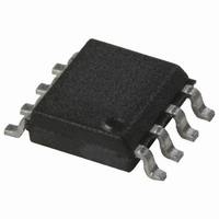
ACSL-6210-00RE Avago Technologies US Inc., ACSL-6210-00RE Datasheet - Page 14

ACSL-6210-00RE
Manufacturer Part Number
ACSL-6210-00RE
Description
OPTOCOUPLER DUAL BI 15MBD 8-SOIC
Manufacturer
Avago Technologies US Inc.
Datasheet
1.ACSL-6210-00RE.pdf
(19 pages)
Specifications of ACSL-6210-00RE
Package / Case
8-SOIC (0.154", 3.90mm Width)
Voltage - Isolation
2500Vrms
Number Of Channels
2, Bi-Directional
Current - Output / Channel
50mA
Data Rate
15MBd
Propagation Delay High - Low @ If
44ns @ 8mA
Current - Dc Forward (if)
15mA
Input Type
DC
Output Type
Open Collector
Mounting Type
Surface Mount
Isolation Voltage
2500 Vrms
Maximum Continuous Output Current
50 mA
Maximum Fall Time
0.012 us
Maximum Forward Diode Current
15 mA
Minimum Forward Diode Voltage
1.25 V
Output Device
Logic Gate Photo IC
Configuration
2 Channel
Maximum Baud Rate
15 MBd(Typ)
Maximum Forward Diode Voltage
1.8 V
Maximum Reverse Diode Voltage
5 V
Maximum Power Dissipation
60 mW
Maximum Operating Temperature
+ 100 C
Minimum Operating Temperature
- 40 C
No. Of Channels
2
Optocoupler Output Type
Logic Gate
Input Current
15mA
Output Voltage
7V
Opto Case Style
SOIC
No. Of Pins
8
Channel Type
Bi-directional
Rohs Compliant
Yes
Lead Free Status / RoHS Status
Lead free / RoHS Compliant
Lead Free Status / RoHS Status
Lead free / RoHS Compliant, Lead free / RoHS Compliant
Other names
516-1602-5
Available stocks
Company
Part Number
Manufacturer
Quantity
Price
Part Number:
ACSL-6210-00RE
Manufacturer:
AVAGO/安华高
Quantity:
20 000
Typical Performance, continued
14
10
150
120
9
8
7
6
5
4
3
2
1
0
Figure 10. Typical supply current per channel vs.
temperature for 5V operation.
90
60
30
-60 -40 -20
0
-60 -40 -20
Figure 13. Typical propagation delay vs.
temperature for 5V operation.
I
I
DDH
F
= 0 mA
T
A
0
t
- TEMPERATURE -°C
T
PHL
t
A
PLH
- TEMPERATURE -°C
0
, R
20
, R
L
L
= 350Ω
20
= 350Ω
40
40
60
I
I
V
DDL
F
DD
= 10 mA
60
80
= 5.0V
V
I
F
DD
100 120
80
= 8.0 mA
= 5.0V
100 120
0.001
1000
0.01
100
40
30
20
10
0.1
10
0
Figure 14. Typical pulse width distortion vs.
temperature for 3.3V operation.
-60 -40 -20
1
1.1
Figure 11. Typical input diode
forward characteristics.
1.2
V
I
F
V
F
+
–
F
T
- FORWARD VOLTAGE - V
A
0
- TEMPERATURE -°C
1.3
20
40
R
L
1.4
= 350Ω
60
T
V
I
F
A
DD
80
= 8.0 mA
= 25°C
1.5
= 3.3V
100 120
1.6
150
120
90
60
30
40
30
20
10
0
0
Figure 12. Typical propagation delay vs.
temperature for 3.3V operation.
Figure 15. Typical pulse width distortion vs.
temperature for 5V operation.
-60 -40 -20
-60 -40 -20
t
t
T
PLH
PHL
T
A
A
0
0
- TEMPERATURE -°C
- TEMPERATURE - °C
, R
, R
L
L
20
20
= 350Ω
= 350Ω
R
40
40
L
= 350Ω
60
60
V
I
F
DD
V
I
= 8.0 mA
80
F
80
DD
= 8.0 mA
= 5.0V
= 3.3V
100 120
100 120


