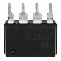
HCPL-3150-000E Avago Technologies US Inc., HCPL-3150-000E Datasheet - Page 18

HCPL-3150-000E
Manufacturer Part Number
HCPL-3150-000E
Description
OPTOCOUPLER 1CH 0.6A 8-DIP
Manufacturer
Avago Technologies US Inc.
Datasheet
1.HCPL-3150.pdf
(21 pages)
Specifications of HCPL-3150-000E
Output Type
Open Collector
Package / Case
8-DIP (0.300", 7.62mm)
Voltage - Isolation
3750Vrms
Number Of Channels
1, Unidirectional
Current - Output / Channel
600mA
Propagation Delay High - Low @ If
300ns @ 7mA ~ 16mA
Current - Dc Forward (if)
25mA
Input Type
DC
Mounting Type
Through Hole
Configuration
1 Channel
Isolation Voltage
3750 Vrms
Maximum Propagation Delay Time
500 ns
Maximum Forward Diode Voltage
1.8 V
Minimum Forward Diode Voltage
1.2 V
Maximum Reverse Diode Voltage
5 V
Maximum Forward Diode Current
25 mA
Maximum Power Dissipation
295 mW
Maximum Operating Temperature
+ 100 C
Minimum Operating Temperature
- 40 C
Number Of Elements
1
Forward Voltage
1.8V
Forward Current
25mA
Package Type
PDIP
Operating Temp Range
-40C to 100C
Power Dissipation
295mW
Propagation Delay Time
500ns
Pin Count
8
Mounting
Through Hole
Reverse Breakdown Voltage
5V
Operating Temperature Classification
Industrial
No. Of Channels
1
Optocoupler Output Type
Gate Drive
Input Current
16mA
Output Voltage
30V
Opto Case Style
DIP
No. Of Pins
8
Common Mode Ratio
15 KV/uS
Rohs Compliant
Yes
Lead Free Status / RoHS Status
Lead free / RoHS Compliant
Lead Free Status / RoHS Status
Lead free / RoHS Compliant, Lead free / RoHS Compliant
Other names
516-1742-5
HCPL-3150-000E
HCPL-3150-000E
Available stocks
Company
Part Number
Manufacturer
Quantity
Price
Company:
Part Number:
HCPL-3150-000E
Manufacturer:
AVAGO
Quantity:
20 000
Part Number:
HCPL-3150-000E
Manufacturer:
AVAGO/安华高
Quantity:
20 000
LED Drive Circuit Considerations for Ultra High CMR Per-
formance
Without a detector shield, the dominant cause of opto-
coupler CMR failure is capacitive coupling from the in-
put side of the optocoupler, through the package, to the
detector IC as shown in Figure 29. The HCPL-3150/315J
improves CMR performance by using a detector IC with
an optically transparent Faraday shield, which diverts
the capaci tively coupled current away from the sensitive
IC circuitry. How ever, this shield does not eliminate the
capacitive coupling between the LED and optocoup ler
pins 5-8 as shown in Figure 30. This capacitive coupling
causes perturbations in the LED current during common
mode transients and becomes the major source of CMR
failures for a shielded optocoupler. The main design ob-
jective of a high CMR LED drive circuit becomes keeping
the LED in the proper state (on or off ) during common
mode transients. For example, the recommended ap-
plication circuit (Figure 25), can achieve 15 kV/μs CMR
while minimizing component complexity.
Techniques to keep the LED in the proper state are dis-
cussed in the next two sections.
CMR with the LED On (CMR
A high CMR LED drive circuit must keep the LED on dur-
ing common mode transients. This is achieved by over-
driving the LED current beyond the input threshold so
that it is not pulled below the threshold during a tran-
sient. A minimum LED cur rent of 10 mA provides ade-
quate margin over the maximum I
15 kV/μs CMR.
18
Figure 27. Energy Dissipated in the HCPL-3150
for Each IGBT Switching Cycle.
7
6
5
4
3
2
1
0
0
Rg – GATE RESISTANCE – Ω
20
40
60
Qg = 100 nC
Qg = 250 nC
Qg = 500 nC
V
V
CC
EE
H
= -9 V
= 19 V
)
80
100
FLH
of 5 mA to achieve
CMR with the LED Off (CMR
A high CMR LED drive circuit must keep the LED off
(V
ple, during a -dV
flowing through C
of the logic gate. As long as the low state voltage devel-
oped across the logic gate is less than V
remain off and no common mode failure will occur.
The open collector drive circuit, shown in Figure 32, can-
not keep the LED off during a +dV
all the current flowing through C
by the LED, and it is not recommended for applications
requiring ultra high CMR
alternative drive circuit which, like the recommended
application circuit (Figure 25), does achieve ultra high
CMR performance by shunting the LED in the off state.
Under Voltage Lockout Feature
The HCPL-3150/315J contains an under voltage lockout
(UVLO) feature that is designed to protect the IGBT under
fault conditions which cause the HCPL-3150/315J supply
voltage (equivalent to the fully-charged IGBT gate volt-
age) to drop below a level necessary to keep the IGBT in
a low resistance state. When the HCPL-3150/315J output
is in the high state and the supply voltage drops below
the HCPL-3150/315J V
the optocoupler output will go into the low state with
a typical delay, UVLO Turn Off Delay, of 0.6 μs. When the
HCPL-3150/315J output is in the low state and the supply
voltage rises above the HCPL-3150/315J V
(11.0 < V
state (assuming LED is “ON”) with a typical delay, UVLO
TURN On Delay, of 0.8 μs.
F
≤ V
F(OFF)
UVLO+
) during common mode transients. For exam-
< 13.5), the optocoupler will go into the high
CM
LEDP
/dt transient in Figure 31, the current
also flows through the R
UVLO-
L
L
performance. Figure 33 is an
)
threshold (9.5 <V
LEDN
CM
/dt transient, since
must be supplied
F(OFF)
UVLO+
, the LED will
UVLO-
SAT
threshold
and V
<12.0),
SAT


