LM8342SD/NOPB National Semiconductor, LM8342SD/NOPB Datasheet - Page 3
LM8342SD/NOPB
Manufacturer Part Number
LM8342SD/NOPB
Description
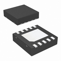
IC PROG TFT CALIBRATOR 10-LLP
Manufacturer
National Semiconductor
Datasheet
1.LM8342SDXNOPB.pdf
(16 pages)
Specifications of LM8342SD/NOPB
Applications
*
Mounting Type
Surface Mount
Package / Case
10-LLP
Lead Free Status / RoHS Status
Lead free / RoHS Compliant
Other names
LM8342SD
LM8342SDTR
LM8342SDTR


OUT
AV
WP
WP
GND
V
SDA
SCL
SCL-S
SET
DAP
DD
Note 1: Absolute Maximum Ratings indicate limits beyond which damage to the device may occur. Operating Ratings indicate conditions for which the device is
intended to be functional, but specific performance is not guaranteed. For guaranteed specifications and test conditions, see the Electrical Characteristics tables.
Note 2: Human Body Model is 1.5 kΩ in series with 100 pF. Machine Model is 0Ω in series with 200 pF.
Note 3: The maximum power dissipation is a function of T
P
Note 4: Programming temperature range 0°C to 70°C .
Note 5: When AV
to 18V, the supply voltage V
Note 6: Electrical Table values apply only for factory testing conditions at the temperature indicated. Factory testing conditions result in very limited self-heating
of the device such that T
T
Note 7: All limits are guaranteed by design or statistical analysis.
Note 8: Typical values represent the parametric norm at the time of characterization.
Note 9: On-Chip Pull Down Resistor of 30 kΩ.
Connection Diagram
Pin Descriptions
DD
D
A
Pin Name
N
P
.
= (T
J(MAX)
— T
A
DD
)/ θ
is in the voltage range of 4.5V to 13V, the supply voltage V
JA
. All numbers apply for packages soldered directly onto a PC board.
J
= T
Pin #
DD
10
1
2
3
4
5
6
7
8
9
A
. No guarantee of parametric performance is indicated in the electrical tables under conditions of internal self-heating where T
is limited to the 2.6V to 3.6V range
Current sink output, adjustable in 128 steps. See Application Section for details.
Analog reference voltage input
Write protect (input)
Inverted WP
Ground
Supply voltage
I
I
Switched SCL connection. Serial clock input when WP
Maximum output current adjustment pin (see block diagram)
Left floating or connect to GND
2
2
C compatible serial data input/output
C compatible serial clock input
WP
WP
N
N
= High
= Low
N
J(MAX)
(output)
, θ
JA
and T
READ (I
10-Pin LLP
Top View
A
yes
yes
. The maximum allowable power dissipation at any ambient temperature is
3
DD
2
C)
can be in 2.25V to 3.6V range. When AV
WRITE
20139202
Function
yes
yes
→
Reg
N
is set to high
WRITE
DD
yes
no
is in the voltage range from 13V
→
EE
SCL Switch
www.national.com
closed
open
J
>
Related parts for LM8342SD/NOPB
Image
Part Number
Description
Manufacturer
Datasheet
Request
R

Part Number:
Description:
IC,Digital Potentiometer,LLCC,10PIN,PLASTIC
Manufacturer:
National Semiconductor
Part Number:
Description:
National Semiconductor [8-Bit D/A Converter]
Manufacturer:
National Semiconductor
Datasheet:
Part Number:
Description:
National Semiconductor [Media Coprocessor]
Manufacturer:
National Semiconductor
Datasheet:
Part Number:
Description:
Digitally Controlled Tone and Volume Circuit with Stereo Audio Power Amplifier, Microphone Preamp Stage and National 3D Sound
Manufacturer:
National Semiconductor
Datasheet:
Part Number:
Description:
Digitally Controlled Tone and Volume Circuit with Stereo Audio Power Amplifier, Microphone Preamp Stage and National 3D Sound
Manufacturer:
National Semiconductor
Datasheet:
Part Number:
Description:
AC97 Rev 2 Codec with Sample Rate Conversion and National 3D Sound
Manufacturer:
National Semiconductor
Part Number:
Description:
Manufacturer:
National Semiconductor
Datasheet:
Part Number:
Description:
Manufacturer:
National Semiconductor
Datasheet:
Part Number:
Description:
General Purpose, Low Voltage, Low Power, Rail-to-Rail Output Operational Amplifiers
Manufacturer:
National Semiconductor
Datasheet:
Part Number:
Description:
8-bit 20 MSPS flash A/D converter.
Manufacturer:
National Semiconductor
Datasheet:
Part Number:
Description:
Low Noise Quad Operational Amplifier
Manufacturer:
National Semiconductor
Datasheet:
Part Number:
Description:
Quad Differential Line Receivers
Manufacturer:
National Semiconductor
Datasheet:
Part Number:
Description:
Quad High Speed Trapezoidal? Bus Transceiver
Manufacturer:
National Semiconductor
Datasheet:
Part Number:
Description:
Dual Line Receiver
Manufacturer:
National Semiconductor
Datasheet: