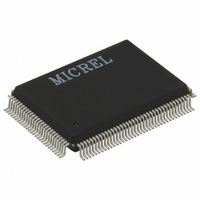
KSZ8995XA Micrel Inc, KSZ8995XA Datasheet - Page 15

KSZ8995XA
Manufacturer Part Number
KSZ8995XA
Description
IC SWITCH 10/100 5PORT 128PQFP
Manufacturer
Micrel Inc
Specifications of KSZ8995XA
Applications
*
Mounting Type
Surface Mount
Package / Case
128-MQFP, 128-PQFP
Number Of Primary Switch Ports
5
Internal Memory Buffer Size
64
Operating Supply Voltage (typ)
1.8/2.5/3.3V
Fiber Support
Yes
Integrated Led Drivers
Yes
Phy/transceiver Interface
MII/SNI
Power Supply Type
Analog/Digital
Package Type
PQFP
Data Rate (typ)
10/100Mbps
Vlan Support
Yes
Operating Temperature (max)
70C
Operating Temperature (min)
0C
Pin Count
128
Mounting
Surface Mount
Jtag Support
No
Operating Temperature Classification
Commercial
Lead Free Status / RoHS Status
Lead free / RoHS Compliant
For Use With
576-1642 - BOARD EVALUATION FOR KSZ8995XA
Lead Free Status / RoHS Status
Compliant, Lead free / RoHS Compliant
Other names
576-1042
Available stocks
Company
Part Number
Manufacturer
Quantity
Price
Company:
Part Number:
KSZ8995XA
Manufacturer:
MICREL
Quantity:
1 334
Company:
Part Number:
KSZ8995XA
Manufacturer:
MICREL30
Quantity:
348
Part Number:
KSZ8995XA
Manufacturer:
MICREL
Quantity:
20 000
September 2008
Notes:
1.
Pin Number
107
108
114
113
P = Power supply.
I = Input.
O = Output.
I/O = Bidirectional.
Gnd = Ground.
Ipu = Input w/internal pull-up.
Ipd = Input w/internal pull-down.
Ipd/O = Input w/internal pull-down during reset, output pin otherwise.
Ipu/O = Input w/internal pull-up during reset, output pin otherwise.
96
95
94
93
92
91
90
45
46
68
67
60
65
64
63
62
61
66
57
55
54
53
52
51
56
NC / MUX1
NC / MUX2
Pin Name
PMRXDV
PMRXER
PMRXD0
PMRXD1
PMRXD2
PMRXD3
PMTXEN
PMTXER
PMTXD0
PMTXD1
PMTXD2
PMTXD3
PMRXC
PMTXC
LED3-2
LED4-0
LED4-1
LED4-2
LED5-0
LED5-1
LED5-2
PCRS
PCOL
MDIO
MDC
PS0
PS1
Type
Ipu/O
Ipu/O
Ipu/O
Ipu/O
Ipu/O
Ipu/O
Ipu/O
Ipu/O
Ipd/O
Ipd/O
Ipd/O
Ipd/O
Ipd/O
Ipd/O
Ipd/O
Ipd/O
Ipu
Ipd
Ipd
Ipd
Ipd
Ipd
Ipd
Ipd
Ipd
O
O
(1)
Port
All
All
3
4
4
4
5
5
5
5
5
5
5
5
5
5
5
5
5
5
5
5
5
5
5
I
I
Pin Function
LED indicator 2.
LED indicator 0.
LED indicator 1.
LED indicator 2.
LED indicator 0.
LED indicator 1. Strap option: PU (default): enable PHY MII I/F Pd:
tristate all PHY MII output. See “Pin# 86 SCONF1.”
LED indicator 2. Aging setup. See “Aging” section.
Switch or PHY[5] MII management data clock.
Switch or PHY[5] MII management data I/O.
No connect. Factory test pin.
No connect. Factory test pin.
PHY[5] MII collision detect/ strap option for port 4 only. PD (default) =
no force flow control, normal operation. PU = force flow control. Refer
to Register 66.
PHY[5] MII carrier sense/strap option for port 4 only. PD (default) =
force half-duplex if auto-negotiation is disabled or fails. PU = force full-
duplex if auto negotiation is disabled or fails. Refer to Register 76.
PHY[5] MII receive clock. PHY mode MII.
PHY[5] MII receive bit 0. Strap option: PD (default) = disable
aggressive back-off algorithm in half-duplex mode; PU = enable for
performance enhancement.
PHY[5] MII receive bit 1. Strap option: PD (default) = drop excessive
collision packets; PU = does not drop excessive collision packets.
PHY[5] MII receive bit 2. Strap option: PD (default) = disable back
pressure; PU = enable back pressure.
PHY[5] MII receive bit 3. Strap option: PD (default) = enable flow
control; PU = disable flow control.
PHY[5] MII receive data valid.
PHY[5] MII receive error. Strap option: PD (default) = packet size 1518/
1522 bytes; PU = 1536 bytes.
PHY[5] MII transmit clock. PHY mode MII.
PHY[5] MII transmit bit 0.
PHY[5] MII transmit bit 1.
PHY[5] MII transmit bit 2.
PHY[5] MII transmit bit 3.
PHY[5] MII transmit enable.
PHY[5] MII transmit error.
No connect or pull down.
No connect or pull down.
15
(2)
2.
PU = Strap pin pull-up.
PD = Strap pull-down.
M9999-091508


