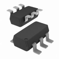
NCP1729SN35T1G ON Semiconductor, NCP1729SN35T1G Datasheet - Page 21

NCP1729SN35T1G
Manufacturer Part Number
NCP1729SN35T1G
Description
IC INVERTER SWITCHED CAP 6TSOP
Manufacturer
ON Semiconductor
Type
Switched Capacitor (Charge Pump), Invertingr
Datasheet
1.NCP1729SN35T1.pdf
(22 pages)
Specifications of NCP1729SN35T1G
Internal Switch(s)
Yes
Synchronous Rectifier
No
Number Of Outputs
1
Voltage - Output
-1.15 ~ -5.5 V, 2.3 ~ 11 V
Current - Output
50mA
Frequency - Switching
35kHz
Voltage - Input
1.15 ~ 5.5 V
Operating Temperature
-40°C ~ 85°C
Mounting Type
Surface Mount
Package / Case
SC-74-6
Power - Output
313mW
Function
Inverting
Output Voltage
- 5.5 V to - 1.15 V
Output Current
100 mA
Maximum Operating Temperature
+ 150 C
Mounting Style
SMD/SMT
Operating Supply Voltage (min)
1.15V
Operating Supply Voltage (max)
5.5V
Package Type
TSOP
Pin Count
6
Mounting
Surface Mount
Lead Free Status / RoHS Status
Lead free / RoHS Compliant
Other names
NCP1729SN35T1GOS
NCP1729SN35T1GOS
NCP1729SN35T1GOSTR
NCP1729SN35T1GOS
NCP1729SN35T1GOSTR
Available stocks
Company
Part Number
Manufacturer
Quantity
Price
Part Number:
NCP1729SN35T1G
Manufacturer:
ON/安森美
Quantity:
20 000
constructed by incorporating combinations of the former circuits. The converter shown above combines Figures 26 and 32 to
form a regulated negative output inverter with a non−regulated positive output doubler. The magnitude of −V
by the resistor values and follows the relationship −V
its output voltage will increase as the negative output load increases. This cross regulation characteristic is shown in the upper
portion of Figure 50. The dashed line is the open loop and the solid line is the closed loop configuration for the load regulation.
The load regulation for the positive doubler with a constant load on the −V
All of the previously shown converter circuits have only single outputs. Applications requiring multiple outputs can be
−3.0
−4.0
−5.0
9.0
8.0
0
Figure 49. Combination of a Closed Loop Negative Inverter with a Positive Output Voltage Doubler
I
Negative Inverter
out
Figure 50. Load Regulation, Output Voltage
, NEGATIVE INVERTER OUTPUT CURRENT (mA)
V
in
vs. Output Current
10
SHDN
Figure 52. Inverter Circuit Board Layout, Top View Copper Side
GND
+
V
R
R
R1 = 10 k, R2 = 20 k
T
in
A
out
out
= 25°C
= 45 W − Open Loop
= 2 W − Closed Loop
1
2
3
Capacitors = 10 mF
Positive Doubler
I
out
20
= 15 mA
OSC
C
+
3
Inverter Size = 0.5 in x 0.2 in
Area = 0.10 in
http://onsemi.com
ref
IC1
6
5
4
(R
NCP1729
2
0.5″
30
/R
21
1
2
, 64.5 mm
+
+ 1). Since the positive output is not within the feedback loop,
C
+
1
10.0
8.0
7.0
9.0
0
10 k
2
C
I
out
+
Negative Inverter I
R
R
T
Figure 51. Load Regulation, Output Voltage
2
A
1
2
out
R
R
, POSITIVE DOUBLER OUTPUT CURRENT (mA)
+
= 25°C
= 10 kW
= 20 kW
1
2
is shown in Figure 51.
10
+
vs. Output Current
−V
GND
−V
out
out
+
20
out
= 15 mA
+V
out
30
out
40
is controlled
50


