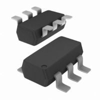
NCP1729SN35T1G ON Semiconductor, NCP1729SN35T1G Datasheet

NCP1729SN35T1G
Specifications of NCP1729SN35T1G
NCP1729SN35T1GOS
NCP1729SN35T1GOSTR
Available stocks
Related parts for NCP1729SN35T1G
NCP1729SN35T1G Summary of contents
Page 1
... Hand Held Instruments This device contains 77 active transistors. Figure 1. Typical Application © Semiconductor Components Industries, LLC, 2006 March, 2006 − Rev. 4 NCP1729SN35T1 NCP1729SN35T1G −V out †For information on tape and reel specifications, 1 http://onsemi.com MARKING DIAGRAM TSOP−6 6 (SOT23−6) 1 EADAYW G SN SUFFIX ...
Page 2
MAXIMUM RATINGS* Rating Á Á Á Á Á Á Á Á Á Á Á Á Á Á Á Á Á Á Input Voltage Range (V to GND) in Á Á Á Á Á Á Á Á Á Á Á Á ...
Page 3
Figure 14 Test Setup T = 25° 1.0 1.5 2.0 2.5 3.0 3 SUPPLY VOLTAGE (V) in Figure 2. Output Resistance vs. Supply Voltage ...
Page 4
Figure 14 Test Setup 2 −1.0 in −2 3 −3 5 −4.0 −5.0 −6 OUTPUT CURRENT (mA) out Figure 8. ...
Page 5
OSC 3 Figure 14. Test Setup/Voltage Inverter DETAILED OPERATING DESCRIPTION The NCP1729 charge pump converter inverts the voltage applied ...
Page 6
Capacitor Selection In order to maintain the lowest output resistance and output ripple voltage recommended that low ESR capacitors be used. Additionally, larger values of C lower the output resistance and larger values of C reduce output voltage ...
Page 7
The NCP1729 primary function is a voltage inverter. The device will convert 5.0 V into −5.0 V with light loads. Two capacitors are required for the inverter to function. A third capacitor, the input bypass capacitor, may be required ...
Page 8
Figure 20. Cascaded Devices for Increased Negative Output Voltage Two or more devices can be cascaded for increased output voltage. Under light load conditions, the output voltage is approximately equal to −V times the number of ...
Page 9
single device can be used to construct a negative voltage doubler. The output voltage is approximately equal to −2.0 V minus the forward voltage drop of each external diode. The performance characteristics for the above converter ...
Page 10
Capacitors = 3 single device can be used to construct a negative voltage tripler. The output voltage is approximately equal to −3.0 V minus the forward voltage drop of each external diode. ...
Page 11
single device can be used to construct a positive voltage doubler. The output voltage is approximately equal to 2.0 V minus the forward voltage drop of each external diode. The performance characteristics for the above converter ...
Page 12
Capacitors = 3 single device can be used to construct a positive voltage tripler. The output voltage is approximately equal to 3.0 V the forward voltage drop of each external diode. The performance characteristics for ...
Page 13
Figure 30. Load Regulated Negative Output Voltage A zener diode can be used with the shutdown input to provide closed loop regulation performance. This significantly reduces the converter’s output resistance and dramatically enhances the load regulation. For ...
Page 14
Figure 32. Line and Load Regulated Negative Output Voltage An adjustable shunt regulator can be used with the shutdown input to give excellent closed loop regulation performance. The shunt regulator acts as a comparator with a precise ...
Page 15
Figure 35. Paralleling Devices for Increased Negative Output Current An increase in converter output current capability with a reduction in output resistance can be obtained by paralleling two or more devices. The output current ...
Page 16
− out Figure 37. External Switch for Increased Negative Output Current The output current capability of the NCP1729 can be extended beyond 600 mA with the addition of two external switch transistors and ...
Page 17
Figure 39. Line and Load Regulated Negative Output Voltage with High Current Capability This converter is a combination of Figures 37 and 32. It provides a line and load regulated output of −2. ...
Page 18
Figure 42. Positive Output Voltage Doubler with High Current Capability The NCP1729 can be configured to produce a positive output voltage doubler with current capability of 500 mA. This is accomplished with ...
Page 19
Figure 44. Line and Load Regulated Positive Output Voltage Doubler with High Current Capability This converter is a combination of Figures 42 and the shunt regulator to close the loop. In this ...
Page 20
single device can be used to split a negative input voltage. The output voltage is approximately equal to −V performance characteristics are shown below. Note that the converter has an output resistance −1.5 −1.7 ...
Page 21
Figure 49. Combination of a Closed Loop Negative Inverter with a Positive Output Voltage Doubler All of the previously shown converter circuits have only single outputs. Applications requiring multiple outputs can be constructed by ...
Page 22
... Pb−Free strategy and soldering details, please download the ON Semiconductor Soldering and Mounting Techniques Reference Manual, SOLDERRM/D. ON Semiconductor and are registered trademarks of Semiconductor Components Industries, LLC (SCILLC). SCILLC reserves the right to make changes without further notice to any products herein ...


