NCP3101BMNTXG ON Semiconductor, NCP3101BMNTXG Datasheet - Page 13
NCP3101BMNTXG
Manufacturer Part Number
NCP3101BMNTXG
Description
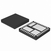
IC CONV VOLT SYNC BUCK 6A 40-QFN
Manufacturer
ON Semiconductor
Type
Step-Down (Buck)r
Datasheet
1.NCP3101BMNTXG.pdf
(26 pages)
Specifications of NCP3101BMNTXG
Internal Switch(s)
Yes
Synchronous Rectifier
Yes
Number Of Outputs
1
Voltage - Output
Adj to 0.8V
Current - Output
6A
Frequency - Switching
275kHz
Voltage - Input
4.5 ~ 13.2 V
Operating Temperature
-40°C ~ 85°C
Mounting Type
Surface Mount
Package / Case
40-TQFN Exposed Pad
Power - Output
3W
Lead Free Status / RoHS Status
Lead free / RoHS Compliant


I
I
ra
I
I
ra
be rounded to 5.6 mH. The inductor should support an RMS
current of 6.02 A and a peak current of 6.78 A.
mechanical and electrical considerations. From a
mechanical perspective, smaller inductor values generally
correspond to smaller physical size. Since the inductor is
often one of the largest components in the regulation system,
a minimum inductor value is particularly important in space
constrained applications. From an electrical perspective, the
maximum current slew rate through the output inductor for
a buck regulator is given by Equation 9.
L
V
V
regulator’s ability to slew current through the output
inductor in response to output load transients. Consequently,
output capacitors must supply the load current until the
inductor current reaches the output load current level.
Reduced inductance to increase slew rates results in larger
values of output capacitance to maintain tight output voltage
regulation. In contrast, smaller values of inductance increase
the regulator’s maximum achievable slew rate and decrease
the necessary capacitance at the expense of higher ripple
current. The peak−to−peak ripple current is given by the
following equation:
D
F
OUT
RMS
OUT
PK
SW
OUT
I
SlewRate
CC
OUT
A standard inductor should be found so the inductor will
The final selection of an output inductor has both
Equation 9 implies that larger inductor values limit the
PK
+ I
OUT
LOUT
1.56 A +
I
PP
* 1 )
6.02 A + 6 A *
= Output current
= Inductor RMS current
= Ripple current ratio
= Output current
= Inductor peak current
= Ripple current ratio
= Output inductance
= Input voltage
= Output voltage
= Duty ratio
= Switching frequency
I
+
+
RMS
V
V
L
OUT
ra
OUT
CC
3.3 V 1 * 27.5%
2
5.6 mH * 275 kHz
+ I
L
* V
OUT
³ 6.78 A + 6.0 A * 1 )
1 * D
OUT
* F
SW
OUT
*
³
1 )
³ 1.56 A +
1 )
26%
ra
12
12
2
³
2
12 V * 3.3 V
5.6 mH
26%
(eq. 10)
2
(eq. 7)
(eq. 8)
(eq. 9)
http://onsemi.com
13
I
L
V
increases as L
between dynamic response and ripple current.
categories: copper and core losses. Copper losses can be
further categorized into DC losses and AC losses. A good
first order approximation of the inductor losses can be made
using the DC resistance as shown below:
I
DCR
LP
geometry of the selected core, core material, and wire used.
Most vendors will provide the appropriate information to
make accurate calculations of the power dissipation, at
which point the total inductor losses can be captured by the
equation below:
LP
LP
LP
Output Capacitor Selection
output capacitor are DC voltage rating, ripple current rating,
output ripple voltage requirements, and transient response
requirements.
current at full load with proper derating. The RMS ratings
given in datasheets are generally for lower switching
frequency than used in switch mode power supplies, but a
multiplier is usually given for higher frequency operation.
The RMS current for the output capacitor can be calculated
below:
Co
I
ra
combination of the ripple current selected, the output
capacitance selected, the Equivalent Series Inductance
(ESL), and Equivalent Series Resistance (ESR).
to the ESR of the output capacitor and the capacitance
selected, which can be calculated as shown in Equation 14:
PP
RMS
OUT
OUT
CO
OUT
From Equation 10 it is clear that the ripple current
The power dissipation of an inductor falls into two
The core losses and AC copper losses will depend on the
The important factors to consider when selecting an
The output capacitor must be rated to handle the ripple
The maximum allowable output voltage ripple is a
The main component of the ripple voltage is usually due
LP
CU_DC
CU_DC
CU_AC
Core
RMS
204 mW + 199 mW ) 2 mW ) 3 mW
RMS
CU_DC
LP
tot
+ I
+ LP
+ I
OUT
= Peak−to−peak current of the inductor
= Output inductance
= Output voltage
= Inductor RMS current
= Inductor DC resistance
= Inductor DC power dissipation
= Inductor DC power dissipation
= Inductor AC power dissipation
= Inductor core power dissipation
= Output capacitor RMS current
= Output current
= Ripple current ratio
OUT
RMS
CU_DC
ra
12
decreases, emphasizing the trade−off
2
³ 0.45 A + 6.0 A
* DCR ³ 199 mW + 6.02
) LP
CU_AC
) LP
26%
12
Core
³
2
* 5.5 mW
(eq. 12)
(eq. 13)
(eq. 11)
Related parts for NCP3101BMNTXG
Image
Part Number
Description
Manufacturer
Datasheet
Request
R

Part Number:
Description:
Wide Input Voltage Synchronous Buck Converter
Manufacturer:
ON Semiconductor
Datasheet:
Part Number:
Description:
ON Semiconductor [VOLTAGE REGULATOR]
Manufacturer:
ON Semiconductor
Datasheet:
Part Number:
Description:
357-036-542-201 CARDEDGE 36POS DL .156 BLK LOPRO
Manufacturer:
ON Semiconductor
Datasheet:
Part Number:
Description:
357-036-542-201 CARDEDGE 36POS DL .156 BLK LOPRO
Manufacturer:
ON Semiconductor
Datasheet:
Part Number:
Description:
357-036-542-201 CARDEDGE 36POS DL .156 BLK LOPRO
Manufacturer:
ON Semiconductor
Datasheet:
Part Number:
Description:
357-036-542-201 CARDEDGE 36POS DL .156 BLK LOPRO
Manufacturer:
ON Semiconductor
Datasheet:
Part Number:
Description:
357-036-542-201 CARDEDGE 36POS DL .156 BLK LOPRO
Manufacturer:
ON Semiconductor
Datasheet:
Part Number:
Description:
357-036-542-201 CARDEDGE 36POS DL .156 BLK LOPRO
Manufacturer:
ON Semiconductor
Datasheet:
Part Number:
Description:
357-036-542-201 CARDEDGE 36POS DL .156 BLK LOPRO
Manufacturer:
ON Semiconductor
Datasheet:
Part Number:
Description:
357-036-542-201 CARDEDGE 36POS DL .156 BLK LOPRO
Manufacturer:
ON Semiconductor
Datasheet:
Part Number:
Description:
357-036-542-201 CARDEDGE 36POS DL .156 BLK LOPRO
Manufacturer:
ON Semiconductor
Datasheet:
Part Number:
Description:
357-036-542-201 CARDEDGE 36POS DL .156 BLK LOPRO
Manufacturer:
ON Semiconductor
Datasheet:
Part Number:
Description:
Manufacturer:
ON Semiconductor
Datasheet:
Part Number:
Description:
Manufacturer:
ON Semiconductor
Datasheet: