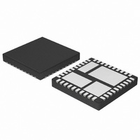
NCP3101BMNTXG ON Semiconductor, NCP3101BMNTXG Datasheet

NCP3101BMNTXG
Specifications of NCP3101BMNTXG
Related parts for NCP3101BMNTXG
NCP3101BMNTXG Summary of contents
Page 1
... RSET (EP) AGND CC Figure 1. Typical Application Diagram This document contains information on a product under development. ON Semiconductor reserves the right to change or discontinue this product without notice. © Semiconductor Components Industries, LLC, 2010 October, 2010 − Rev See detailed ordering and shipping information in the package dimensions section on page 24 of this data sheet ...
Page 2
VCC 13 FB POR UVLO − 0.8 V ref CLOCK COMP DIS RAMP 17 − FAULT + 400 −550 mV VOCTH CPHS FAULT FAULT − PWM OUT S OSC FAULT OSC ...
Page 3
Table 1. PIN FUNCTION DESCRIPTION Pin No Symbol 1−4, 36−40 PWRPHS 5−12 PWRGND 13 VCC 14,15,19,20,23 AGND COMP/DIS TGOUT 22 CPHS 24 BST 25 TGIN 26−34 PWRVCC 35 BG Table 2. ABSOLUTE MAXIMUM RATINGS ...
Page 4
Table 2. ABSOLUTE MAXIMUM RATINGS Pin Name Bootstrap Pin Voltage vs V PWRPHS High Side Switch Max DC Current V Pin Voltage PWRPHS V Pin Voltage (spikes < 50 ns) PWRPHS CPHASE Pin Voltage CPHASE Pin Voltage (spikes < 50 ...
Page 5
Table 3. ELECTRICAL CHARACTERISTICS for min/max values unless otherwise noted). Characteristic Power Power Channel Input Voltage Range Boost Voltage Range SUPPLY CURRENT Quiescent Supply Current Quiescent Supply Current V Supply Current CC V Supply Current CC Boost Quiescent Current Shutdown ...
Page 6
TYPICAL OPERATING CHARACTERISTICS 285 284 283 282 281 280 12 V 279 278 5 V 277 276 275 −40 − JUNCTION TEMPERATURE (°C) J Figure 5. Frequency (F Temperature 0.807 0.805 0.803 0.801 0.799 ...
Page 7
TYPICAL OPERATING CHARACTERISTICS −40 − JUNCTION TEMPERATURE (°C) J Figure 11. I vs. ...
Page 8
TYPICAL OPERATING CHARACTERISTICS −40 − JUNCTION TEMPERATURE (°C) Figure 17. Minimum Duty Cycle vs. Temperature http://onsemi.com 8 80 100 120 ...
Page 9
General NCP3101C is a high efficiency integrated wide input voltage 6 A synchronous PWM buck converter designed to operate from a 4 13.2 V supply. The output voltage of the converter can be precisely regulated down to 800 ...
Page 10
Normal Shutdown Behavior Normal shutdown occurs when the IC stops switching because the input supply reaches UVLO threshold. In this case, switching stops, the internal soft start, SS, is discharged, and all gate pins go low. The switch node enters ...
Page 11
LS Gate Drive 2V BG Comparator 2V HS Gate Drive Switch Node Comparator 2V Switch Node SCP Trip Voltage C Phase SCP Comparator/ Latch Output Figure 24. Switching and Current Limit Timing Overcurrent Threshold Setting The NCP3101C overcurrent threshold can ...
Page 12
... ON Semiconductor has a Microsoft Excel® based design tool available online under the design tools section of the NCP3101C product page. The tool allows you to capture your design point and optimize the performance of your regulator based on your design criteria ...
Page 13
RMS OUT 26% 6. Output current OUT I = Inductor RMS current RMS ra = Ripple current ratio ...
Page 14
ESR_C OUT ESR 19 26 275 kHz * 820 Output capacitor ESR ESR C = Output capacitance ...
Page 15
Table 5. TRANSIENT RESPONSE VERSUS OUTPUT CAPACITANCE (50% to 100% Load Step) Drop (mV) COUT OS−CON (mF) 0 384 100 224 150 192 220 164 270 156 560 128 820 112 1000 112 Figure 27. Typical Waveform of Transient Response ...
Page 16
P = High side MOSFET total switching SW_TOT losses The first term for total switching losses from Equation 24 are the losses associated with turning the high−side MOSFET on and off and the corresponding overlap in drain voltage and current. ...
Page 17
MOSFET turning off and the high−side MOSFET turning on, typically Low−side MOSFET body diode losses BODY V = Body diode forward voltage drop FD Control Dissipation The control portion of the IC power dissipation is determined ...
Page 18
... The values can be adjusted in real time using the compensation tool comp calc, available for download at ON Semiconductor’s website. The poles of the compensation network are calculated as follows reduced to zero. The first pole is set at the ESR zero. ...
Page 19
In practical design, the feed through resistor should the value minimize error from high frequency feed 2 through noise. Using the 2X assumption and the feed through capacitor can be calculated ...
Page 20
The cross over combined compensation network can be used to calculate the transconductance output compensation network as follows ³ 43.3 nF ...
Page 21
ICinrush_PK CIN ESR 12 120 CIN 0.316 * ICin_RMS CINESR 0 330 mF 5. 0.316 * 0.1 ...
Page 22
Output Voltage Output Current t tss Figure 35. Voltage Enable Load Current If the inrush current is higher than the steady state input current during max load, then an input fuse should be rated 2 accordingly using I t ...
Page 23
RLO8 PWRVCC BG PWRPHS Figure 36. Schematic Diagram of NCP3101C Evaluation Board http://onsemi.com 23 NC COMP FB AGND AGND VCC PWRGND PWRGND PWRGND ...
Page 24
ORDERING INFORMATION Device NCP3101CMNTXG †For information on tape and reel specifications, including part orientation and tape sizes, please refer to our Tape and Reel Packaging Specifications Brochure, BRD8011/D. Temperature Grade Package For −40°C to +125°C QFN40 (Pb−Free) http://onsemi.com 24 † ...
Page 25
... BOTTOM VIEW 0.72 0.92 1.58 6.30 2.31 0.92 *For additional information on our Pb−Free strategy and soldering details, please download the ON Semiconductor Soldering and Mounting Techniques Reference Manual, SOLDERRM/D. PACKAGE DIMENSIONS QFN40 6x6, 0.5P CASE 485AK−01 ISSUE A NOTES: 1. DIMENSIONING AND TOLERANCING PER ASME Y14 ...
Page 26
... Opportunity/Affirmative Action Employer. This literature is subject to all applicable copyright laws and is not for resale in any manner. PUBLICATION ORDERING INFORMATION LITERATURE FULFILLMENT: Literature Distribution Center for ON Semiconductor P.O. Box 5163, Denver, Colorado 80217 USA Phone: 303−675−2175 or 800−344−3860 Toll Free USA/Canada Fax: 303− ...


