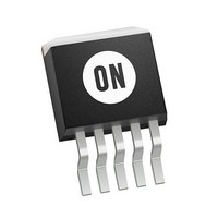
MC33167D2T ON Semiconductor, MC33167D2T Datasheet - Page 8

MC33167D2T
Manufacturer Part Number
MC33167D2T
Description
IC REG SWITCH INVERT 5A D2PAK-5
Manufacturer
ON Semiconductor
Type
Step-Down (Buck), Step-Up (Boost), Invertingr
Datasheet
1.MC33167TG.pdf
(20 pages)
Specifications of MC33167D2T
Internal Switch(s)
Yes
Synchronous Rectifier
No
Number Of Outputs
1
Voltage - Output
5 ~ 40 V
Current - Output
5A
Frequency - Switching
72kHz
Voltage - Input
7.5 ~ 40 V
Operating Temperature
-40°C ~ 85°C
Mounting Type
Surface Mount
Package / Case
D²Pak, TO-263 (5 leads + tab)
Mounting Style
SMD/SMT
Lead Free Status / RoHS Status
Contains lead / RoHS non-compliant
Power - Output
-
Lead Free Status / Rohs Status
Lead free / RoHS Compliant
Available stocks
Company
Part Number
Manufacturer
Quantity
Price
Company:
Part Number:
MC33167D2T
Manufacturer:
ON
Quantity:
347
Company:
Part Number:
MC33167D2T
Manufacturer:
MOT
Quantity:
5 510
Company:
Part Number:
MC33167D2TC
Manufacturer:
TI
Quantity:
5 510
Switch Output
40 V, with a minimum peak collector current of 5.5 A. When
configured for step−down or voltage−inverting applications,
as in Figures 19 and 23, the inductor will forward bias the
output rectifier when the switch turns off. Rectifiers with a
high forward voltage drop or long turn on delay time should
not be used. If the emitter is allowed to go sufficiently
negative, collector current will flow, causing additional
device heating and reduced conversion efficiency. Figure 9
shows that by clamping the emitter to 0.5 V, the collector
current will be in the range of 100 mA over temperature. A
1N5825 or equivalent Schottky barrier rectifier is
recommended to fulfill these requirements.
Undervoltage Lockout
incorporated to guarantee that the integrated circuit is fully
or plug−in prototype boards. Special care should be taken
to separate ground paths from signal currents and ground
paths from load currents. All high current loops should be
kept as short as possible using heavy copper runs to
minimize ringing and radiated EMI. For best operation, a
The output transistor is designed to switch a maximum of
An Undervoltage Lockout comparator has been
Do not attempt to construct a converter on wire−wrap
DESIGN CONSIDERATIONS
MC34167, MC33167
http://onsemi.com
8
functional before the output stage is enabled. The internal
reference voltage is monitored by the comparator which
enables the output stage when V
erratic output switching as the threshold is crossed, 0.9 V of
hysteresis is provided.
Thermal Protection
the integrated circuit in the event that the maximum junction
temperature is exceeded. When activated, typically at 170°C,
the latch is forced into a ‘reset’ state, disabling the output
switch. This feature is provided to prevent catastrophic
failures from accidental device overheating. It is not
intended to be used as a substitute for proper heatsinking.
The MC34167 is contained in a 5−lead TO−220 type package.
The tab of the package is common with the center pin (Pin 3)
and is normally connected to ground.
tight component layout is recommended. Capacitors C
C
to the IC as physically possible. It is also imperative that the
Schottky diode connected to the Switch Output be located as
close to the IC as possible.
O
Internal Thermal Shutdown circuitry is provided to protect
, and all feedback components should be placed as close
CC
exceeds 5.9 V. To prevent
in
,


