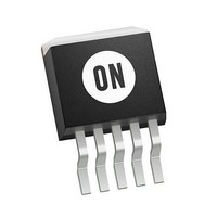
MC33167D2T ON Semiconductor, MC33167D2T Datasheet

MC33167D2T
Specifications of MC33167D2T
Available stocks
Related parts for MC33167D2T
MC33167D2T Summary of contents
Page 1
MC34167, MC33167 5.0 A, Step−Up/Down/ Inverting Switching Regulators The MC34167, MC33167 series are high performance fixed frequency power switching regulators that contain the primary functions required for dc−to−dc converters. This series was specifically designed to be incorporated in step−down and ...
Page 2
MAXIMUM RATINGS (Note 1 and 2) Rating Power Supply Input Voltage Switch Output Voltage Range Voltage Feedback and Compensation Input Voltage Range Power Dissipation Case 314A, 314B and 314D (T = +25°C) A Thermal Resistance, Junction−to−Ambient Thermal Resistance, Junction−to−Case 2 ...
Page 3
ELECTRICAL CHARACTERISTICS temperature range that applies (Notes 4, 5), unless otherwise noted.) Characteristic OSCILLATOR Frequency ( ERROR AMPLIFIER Voltage Feedback Input Threshold Line Regulation ( ...
Page 4
Max = 5.15 V FB(th) 5.17 5.09 V Typ = 5.05 V FB(th) 5.01 V Min = 4.95 V FB(th) 4.93 4.85 − 55 − AMBIENT TEMPERATURE ...
Page 5
V CC − 0.5 −1.0 −1.5 − 2.0 − 2.5 − 3.0 0 2.0 4 SWITCH OUTPUT SOURCE CURRENT (A) Source Figure 8. Switch Output Source Saturation versus Source Current 7.2 V Pins ...
Page 6
MC34167, MC33167 + Oscillator C T Pulse Width PWM Latch Modulator Thermal Shutdown 100 mA GND Compensation 3 = Figure 14. MC34167 Representative Block Diagram 4.1 V Timing Capacitor C T Compensation 2 Switch Output OFF Figure 15. ...
Page 7
The MC34167, MC33167 series are monolithic power switching regulators that are optimized for dc−to−dc converter applications. These devices operate as fixed frequency, voltage mode regulators containing all the active functions required to directly implement step−down and voltage−inverting converters with a ...
Page 8
Switch Output The output transistor is designed to switch a maximum with a minimum peak collector current of 5.5 A. When configured for step−down or voltage−inverting applications Figures 19 and 23, the inductor will forward ...
Page 9
Error 100 mA Amp 120 Compensation Standby Mode Figure 16. Low Power Standby Circuit Compensation V in MC34167, MC33167 100 mA 1 Compensation Shutdown Figure 17. Over Voltage Shutdown Circuit + Error 100 ...
Page 10
Oscillator PWM Thermal 3 Test Line Regulation Load Regulation Output Ripple Short Circuit Current Efficiency L = Coilcraft M1496−A or General Magnetics Technology GMT−0223, 42 turns of #16 AWG on Magnetics Inc. 58350−A2 core. Heatsink = AAVID Engineering Inc. ...
Page 11
Oscillator PWM Thermal 3 *Gate resistor R , zener diode D , and diode Test Line Regulation Load Regulation Output Ripple Short Circuit Current Efficiency L = Coilcraft M1496−A or General Magnetics Technology GMT−0223, 42 turns ...
Page 12
Oscillator PWM Thermal 3 Test Line Regulation Load Regulation Output Ripple Short Circuit Current Efficiency L = Coilcraft M1496−A or General Magnetics Technology GMT−0223, 42 turns of #16 AWG on Magnetics Inc. 58350−A2 core. Heatsink = AAVID Engineering Inc. ...
Page 13
Oscillator PWM Thermal 3 Tests Line Regulation 5 −12 V Load Regulation 5 − Output Ripple 5 −12 V Short Circuit Current 5.0 V ...
Page 14
MC34167, MC33167 + Oscillator S R PWM Thermal −12 V 1000 + *Gate resistor R , zener diode D G Test Line Regulation V = − − Load Regulation V = ...
Page 15
RFI 115 VAC Filter + 220 100k Core and Bobbin − Coilcraft PT3595 Primary − 104 turns #26 AWG Base Drive − 3 turns #26 AWG Secondaries ...
Page 16
Calculation Step−Down out ) off sat * V out (Notes off osc t off Duty Cycle t f ...
Page 17
... ORDERING INFORMATION Device MC33167D2T MC33167D2TG MC33167D2TR4 MC33167D2TR4G MC33167T MC33167TG MC33167TH MC33167THG MC33167TV MC33167TVG MC34167D2T MC34167D2TG MC34167D2TR4 MC34167D2TR4G MC34167T MC34167TG MC34167TH MC34167THG MC34167TV MC34167TVG †For information on tape and reel specifications, including part orientation and tape sizes, please refer to our Tape and Reel Packaging Specifications Brochure, BRD8011/D ...
Page 18
B −P− Q OPTIONAL CHAMFER 0.014 (0.356 −P− OPTIONAL Q CHAMFER 0.24 (0.610 0.10 (0.254 MC34167, MC33167 PACKAGE DIMENSIONS ...
Page 19
PACKAGE DIMENSIONS B −Q− DETAIL A− 0.356 (0.014 MC34167, MC33167 TO−220 T SUFFIX CASE 314D−04 ISSUE F SEATING NOTES: −T− PLANE 1. DIMENSIONING ...
Page 20
... Pb−Free strategy and soldering details, please download the ON Semiconductor Soldering and Mounting Techniques Reference Manual, SOLDERRM/D. ON Semiconductor and are registered trademarks of Semiconductor Components Industries, LLC (SCILLC). SCILLC reserves the right to make changes without further notice to any products herein ...


