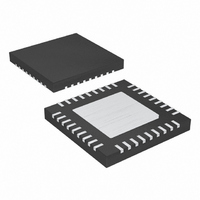
MAX8654ETX+T Maxim Integrated Products, MAX8654ETX+T Datasheet - Page 15

MAX8654ETX+T
Manufacturer Part Number
MAX8654ETX+T
Description
IC REG STP DWN 12V 8A 36TQFN
Manufacturer
Maxim Integrated Products
Type
Step-Down (Buck)r
Datasheet
1.MAX8654ETX.pdf
(17 pages)
Specifications of MAX8654ETX+T
Internal Switch(s)
Yes
Synchronous Rectifier
No
Number Of Outputs
1
Voltage - Output
0.6 ~ 11.9 V
Current - Output
8A
Frequency - Switching
250kHz ~ 1.2MHz
Voltage - Input
4.5 ~ 14 V
Operating Temperature
-40°C ~ 85°C
Mounting Type
Surface Mount
Package / Case
36-TQFN Exposed Pad
Power - Output
2.86W
Lead Free Status / RoHS Status
Lead free / RoHS Compliant
The above equations provide accurate compensation
when the zero-cross frequency is significantly higher
than the double-pole frequency. When the zero-cross
frequency is near the double-pole frequency, the actual
zero-cross frequency is higher than the calculated fre-
quency. In this case, lowering the value of R1 reduces the
zero-cross frequency. Also, set the third pole of the type 3
compensation close to the switching frequency if the
zero-cross frequency is above 200kHz to boost the phase
margin. Note that the value of R4 can be altered to make
the values of the compensation components practical.
The recommended range for R3 is 2kΩ to 10kΩ.
Careful PCB layout is critical to achieve clean and sta-
ble operation. It is highly recommended to duplicate
the MAX8654 EV kit layout for optimum performance. If
deviation is necessary, follow these guidelines for good
PCB layout:
Figure 4. Transfer Function for Type 3 Compensation
PCB Layout Considerations and Thermal
TRANSFER FUNCTION
POWER-STAGE
______________________________________________________________________________________
COMPENSATION
TRANSFER
FUNCTION
Performance
SECOND ZEROS
FIRST AND
DOUBLE POLE
f
1) Connect input and output capacitors, V
2) Place capacitors on V
3) Keep the high-current paths as short and wide as
4) Connect IN, LX, and PGND separately to a large
5) Ensure all feedback connections are short and
6) Route high-speed switching nodes, such as LX,
capacitors, to the power ground plane; connect all
other capacitors to the signal ground plane.
close as possible to the IC and its corresponding pin
using direct traces. Keep power ground plane (con-
nected to PGND) and signal ground plane (connect-
ed to GND) separate.
possible. Keep the path of switching current short
and minimize the loop area formed by LX, the out-
put capacitors, and the input capacitors.
copper area to help cool the IC to further improve
efficiency and long-term reliability.
direct. Place the feedback resistors and compensa-
tion components as close to the IC as possible.
away from sensitive analog areas (FB, COMP).
Step-Down Regulator
SECOND
POLE
12V, 8A 1.2MHz
OPEN-LOOP
GAIN
ZERO
ESR
VP
, V
THIRD
POLE
IN
, V
VL
, V
VDL
VP
, and SS as
and V
VDL
15


