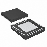
MAX5951ETJ+T Maxim Integrated Products, MAX5951ETJ+T Datasheet - Page 17

MAX5951ETJ+T
Manufacturer Part Number
MAX5951ETJ+T
Description
IC BUCK PWM CTRLR 12V/5V 32-TQFN
Manufacturer
Maxim Integrated Products
Type
Step-Down (Buck)r
Datasheet
1.MAX5951ETJT.pdf
(25 pages)
Specifications of MAX5951ETJ+T
Internal Switch(s)
No
Synchronous Rectifier
No
Number Of Outputs
1
Voltage - Output
0.8 ~ 5.5 V
Current - Output
10A
Frequency - Switching
100kHz ~ 1MHz
Voltage - Input
8 ~ 16 V
Operating Temperature
-40°C ~ 85°C
Mounting Type
Surface Mount
Package / Case
32-TQFN Exposed Pad
Power - Output
2.76W
Lead Free Status / RoHS Status
Lead free / RoHS Compliant
The MAX5951 uses a voltage-mode control scheme
that regulates the output voltage by comparing the
error amplifier output (COMP) with an internal ramp to
produce the required duty cycle. The output lowpass
LC filter creates a double pole at the resonant frequen-
cy, which has a gain drop of -40dB/decade. The com-
pensation network must compensate for this gain drop
and phase shift in order to achieve a stable closed-loop
system.
The basic regulator loop consists of a power modulator,
an output feedback divider, and a voltage-error amplifi-
er. The power modulator has a DC gain set by
V
the output inductance (L), the output capacitance
(C
Below are equations that define the power modulator:
Figure 5. Error-Amplifier Compensation Circuit (Closed-Loop
and Error-Amplifier Gain Plot) for Ceramic Capacitors
IN
OUT
/V
GAIN
RAMP
(dB)
), and its equivalent series resistance (ESR).
V
OUT
, with a double pole and a single zero set by
Compensation Design Guidelines
G
f
f
LC
ZESR
C6
MOD DC
R3
______________________________________________________________________________________
=
CLOSED-LOOP
GAIN
2
R4
(
R6
f
=
Z1
π
2
f
)
Z2
π
L C
=
×
REF
×
1
C
V
f
C
RAMP
OUT
OUT
V
IN
R5
1
f
12V/5V Input Buck PWM Controller
P2
EA
C8
×
f
P3
R
C7
ESR
EA
GAIN
FREQUENCY
COMP
The switching frequency is programmable between
100kHz and 1000kHz by an external resistor at RT. The
crossover frequency (f
the closed-loop gain is equal to unity, should be set to
f
The error amplifier must provide a gain-and-phase
boost to compensate for the rapid gain-and-phase loss
from the LC double pole. This is accomplished by utiliz-
ing type 3 compensation (see Figures 5 and 6) that
introduces two zeros and three poles into the control
loop. The error amplifier has a low-frequency pole (f
at the origin; two zeros at:
and:
and higher frequency poles at:
and:
Figure 6. Error-Amplifier Compensation Circuit (Closed-Loop
and Error-Amplifier Gain Plot) for Higher ESR Output
Capacitors
SW
/ 10 or f
GAIN
(dB)
V
OUT
GBW
C6
/ 25, whichever is lower.
R3
f
f
f
f
P2
P3
Z1
Z2
R4
R6
f
Z1
=
=
=
=
C
f
), which is the frequency when
2
Z2
2
2
2
π
π
π
π
REF
CLOSED-LOOP
GAIN
×
×
×
×
R
R
R
R
1
1
5
1
6
1
3
5
R5
×
×
f
×
×
P2
EA
C8
C
C
C
C
7
6
6
8
f
C
C7
f
P3
FREQUENCY
COMP
EA
GAIN
P1
17
)


