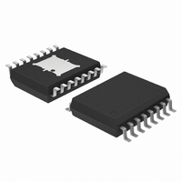
NCP3163PWG ON Semiconductor, NCP3163PWG Datasheet - Page 8

NCP3163PWG
Manufacturer Part Number
NCP3163PWG
Description
IC REG SW DC/DC 3.4A 16SOIC
Manufacturer
ON Semiconductor
Type
Step-Down (Buck), Step-Up (Boost), Invertingr
Datasheet
1.NCP3163BMNR2G.pdf
(20 pages)
Specifications of NCP3163PWG
Internal Switch(s)
Yes
Synchronous Rectifier
No
Number Of Outputs
1
Voltage - Output
Adj to 40V
Current - Output
3.4A
Frequency - Switching
50kHz ~ 300kHz
Voltage - Input
2.5 ~ 40 V
Operating Temperature
0°C ~ 70°C
Mounting Type
Surface Mount
Package / Case
16-SOIC (7.5mm Width) Exposed Pad, 16-eSOIC, 16-HSOIC
Output Voltage
1 V to 40 V
Output Current
3.4 A
Input Voltage
2.5 V to 40 V
Switching Frequency
50 KHz to 1 MHz
Operating Temperature Range
- 40 C to + 85 C
Mounting Style
SMD/SMT
Lead Free Status / RoHS Status
Lead free / RoHS Compliant
Power - Output
-
Lead Free Status / Rohs Status
Lead free / RoHS Compliant
Available stocks
Company
Part Number
Manufacturer
Quantity
Price
Company:
Part Number:
NCP3163PWG
Manufacturer:
ON
Quantity:
141
optimized for DC−to−DC converter applications. The
combination of its features enables the system designer to
directly implement step−up, step−down, and voltage−
inverting converters with a minimum number of external
components. Potential applications include cost sensitive
consumer products as well as equipment for the automotive,
computer, and industrial markets. A representative block
diagram is shown in Figure 2.
off−time voltage mode ripple regulator. In general, this
mode of operation is somewhat analogous to a capacitor
charge pump and does not require dominant pole loop
compensation for converter stability. The Typical Operating
Waveforms are shown in Figure 19. The output voltage
waveform shown is for a step−down converter with the
ripple and phasing exaggerated for clarity. During initial
converter startup, the feedback comparator senses that the
output voltage level is below nominal. This causes the
output switch to turn on and off at a frequency and duty cycle
controlled by the oscillator, thus pumping up the output filter
capacitor. When the output voltage level reaches nominal,
the feedback comparator sets the latch, immediately
terminating switch conduction. The feedback comparator
will inhibit the switch until the load current causes the output
voltage to fall below nominal. Under these conditions,
output switch conduction can be inhibited for a partial
The NCP3163 is a monolithic power switching regulator
The NCP3163 operates as a fixed on−time, variable
Timing Capacitor C
OPERATING DESCRIPTION
Comparator Output
Oscillator Output
Nominal Output
Output Voltage
Output Switch
Voltage Level
0.55 V
1.25 V
T
On
Off
1
0
1
0
Figure 19. Typical Operating Waveforms
t
Startup
http://onsemi.com
INTRODUCTION
9t
8
oscillator cycle, a partial cycle plus a complete cycle,
multiple cycles, or a partial cycle plus multiple cycles.
Oscillator
are programmed by the value selected for timing capacitor
C
internal current source and sink, generating a negative going
sawtooth waveform at Pin 6. As C
pulse is generated at the oscillator output. This pulse is
connected to the NOR gate center input, preventing output
switch conduction, and to the AND gate upper input,
allowing the latch to be reset if the comparator output is low.
Thus, the output switch is always disabled during ramp−up
and can be enabled by the comparator output only at the start
of ramp−down. The oscillator peak and valley thresholds are
1.25 V and 0.55 V, respectively, with a charge current of
225 mA and a discharge current of 25 mA, yielding a
maximum on−time duty cycle of 90%. A reduction of the
maximum duty cycle may be required for specific converter
configurations. This can be accomplished with the addition
of an external deadtime resistor (R
resistor increases the discharge current which reduces the
on−time of the output switch. The converter output can be
inhibited by clamping C
small−signal transistor. To calculate the frequency when
only C
Figure 22. When R
maximum duty cycle can be calculated with the NCP3163
design tool found at www.onsemi.com.
T
The oscillator frequency and on−time of the output switch
. Capacitor C
T
is connected to Pin 6, use the equations found in
Quiescent Operation
T
is charged and discharged by a 9 to 1 ratio
T
is also used, the frequency and
T
to ground with an external NPN
DT
) placed across C
T
charges, an internal
T
. The


