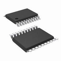
LM26003QMHX/NOPB National Semiconductor, LM26003QMHX/NOPB Datasheet - Page 16

LM26003QMHX/NOPB
Manufacturer Part Number
LM26003QMHX/NOPB
Description
IC REG BUCK LOW IQ 3A 20-TSSOP
Manufacturer
National Semiconductor
Series
PowerWise®r
Type
Step-Down (Buck)r
Datasheet
1.LM26003QMHNOPB.pdf
(20 pages)
Specifications of LM26003QMHX/NOPB
Internal Switch(s)
Yes
Synchronous Rectifier
No
Number Of Outputs
1
Voltage - Output
1.25 ~ 35 V
Current - Output
3A
Frequency - Switching
150kHz ~ 500kHz
Voltage - Input
4 ~ 38 V
Operating Temperature
-40°C ~ 125°C
Mounting Type
Surface Mount
Package / Case
20-TSSOP Exposed Pad, 20-eTSSOP, 20-HTSSOP
Power - Output
3.1W
Lead Free Status / RoHS Status
Lead free / RoHS Compliant
Other names
LM26003QMHX
Available stocks
Company
Part Number
Manufacturer
Quantity
Price
Company:
Part Number:
LM26003QMHX/NOPB
Manufacturer:
NS/TI
Quantity:
350
Part Number:
LM26003QMHX/NOPB
Manufacturer:
TI/德州仪器
Quantity:
20 000
www.national.com
2. Once the fp range is determined, R5 should be calculated
using:
Where B is the desired feedback gain in v/v between fp and
fz, and gm is the transconductance of the error amplifier. A
gain value around 10 dB (3.3v/v) is generally a good starting
point. Bandwidth increases with increasing values of R3.
3. Next, place a zero (fzc) near fp using C5. C5 can be de-
termined with the following equation:
The selected value of C5 should place fzc within a decade
above or below fpmax and not less than fpmin. A higher C5
value (closer to fpmin) generally provides a more stable loop,
but too high a value will slow the transient response time.
Conversely, a smaller C5 value will result in a faster transient
response, but lower phase margin.
4. A second pole (fpc1) can also be placed at fz. This pole can
be created with a single capacitor, C4. The minimum value
for this capacitor can be calculated by:
C4 may not be necessary in all applications. However if the
operating frequency is being synchronized below the nominal
frequency, C4 is recommended. Although it is not required for
stability, C4 is very helpful in suppressing noise.
A phase lead capacitor can also be added to increase the
phase and gain margins. The phase lead capacitor is most
helpful for high input voltage applications or when synchro-
nizing to a frequency greater than nominal. This capacitor,
shown as C11 in
the top feedback resistor, R1.
C11 introduces an additional zero and pole to the compen-
sation network. These frequencies can be calculated as
shown below:
A phase lead capacitor will boost loop phase around the re-
gion of the zero frequency, fzff. fzff should be placed some-
what below the fpz1 frequency set by C4. However, if C11 is
too large, it will have no effect.
PCB Layout
Good board layout is critical for switching regulators such as
the LM26003. First, the ground plane area must be sufficient
for thermal dissipation purposes, and second, appropriate
guidelines must be followed to reduce the effects of switching
noise.
Figure
10, should be placed in parallel with
16
Switch mode converters are very fast switching devices. In
such devices, the rapid increase of input current combined
with parasitic trace inductance generates unwanted Ldi/dt
noise spikes at the SW node and also at the VIN node. The
magnitude of this noise tends to increase as the output current
increases. This parasitic spike noise may turn into electro-
magnetic interference (EMI) and can also cause problems in
device performance. Therefore, care must be taken in layout
to minimize the effect of this switching noise.
The current sensing circuit in current mode devices can be
easily affected by switching noise. This noise can cause duty-
cycle jitter which leads to increased spectrum noise. Although
the LM26003 has 150 ns blanking time at the beginning of
every cycle to ignore this noise, some noise may remain after
the blanking time. Following the important guidelines below
will help minimize switching noise and its effect on current
sensing.
The switch node area should be as small as possible. The
catch diode, input capacitors, and output capacitors should
be grounded to the same local ground, with the bulk input
capacitor grounded as close as possible to the catch diode
anode. Additionally, the ground area between the catch diode
and bulk input capacitor is very noisy and should be some-
what isolated from the rest of the ground plane.
A ceramic input capacitor must be connected as close as
possible to the AVIN pin as well as PVIN pin. The capacitor
between AVIN and ground should be grounded close to the
GND pins of the LM26003 and the PVIN capacitor should be
grounded close to the Schottky diode ground. Often, the AVIN
bypass capacitor is most easily located on the bottom side of
the PCB. It increases trace inductance due to the vias, it re-
duces trace length however.
The above layout recommendations are illustrated below in
Figure
It is a good practice to connect the EP, GND pin, and small
signal components (COMP, FB, FREQ) to a separate ground
plane, shown in
as a signal ground symbol. Both the exposed pad and the
11.
FIGURE 11. Example PCB Layout
Figure 11
as EP GND, and in the schematics
30067632


