LM26003QMHX/NOPB National Semiconductor, LM26003QMHX/NOPB Datasheet - Page 15

LM26003QMHX/NOPB
Manufacturer Part Number
LM26003QMHX/NOPB
Description
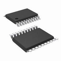
IC REG BUCK LOW IQ 3A 20-TSSOP
Manufacturer
National Semiconductor
Series
PowerWise®r
Type
Step-Down (Buck)r
Datasheet
1.LM26003QMHNOPB.pdf
(20 pages)
Specifications of LM26003QMHX/NOPB
Internal Switch(s)
Yes
Synchronous Rectifier
No
Number Of Outputs
1
Voltage - Output
1.25 ~ 35 V
Current - Output
3A
Frequency - Switching
150kHz ~ 500kHz
Voltage - Input
4 ~ 38 V
Operating Temperature
-40°C ~ 125°C
Mounting Type
Surface Mount
Package / Case
20-TSSOP Exposed Pad, 20-eTSSOP, 20-HTSSOP
Power - Output
3.1W
Lead Free Status / RoHS Status
Lead free / RoHS Compliant
Other names
LM26003QMHX
Available stocks
Company
Part Number
Manufacturer
Quantity
Price
Company:
Part Number:
LM26003QMHX/NOPB
Manufacturer:
NS/TI
Quantity:
350
Part Number:
LM26003QMHX/NOPB
Manufacturer:
TI/德州仪器
Quantity:
20 000
leakage current. Also keep in mind that the reverse leakage
current of a Schottky diode increases with temperature and
with reverse voltage. Reverse voltage equals roughly the in-
put voltage in a buck converter. At hot, the diode reverse
leakage current may be larger than the current consumption
of the LM26003.
COMPENSATION
The purpose of loop compensation is to ensure stable oper-
ation while maximizing dynamic performance. Stability can be
analyzed with loop gain measurements, while dynamic per-
formance is analyzed with both loop gain and load transient
response. Loop gain is equal to the product of control-output
transfer function (power stage) and the feedback transfer
function (the compensation network).
For stability purposes, our target is to have a loop gain slope
that is -20dB /decade from a very low frequency to beyond
the crossover frequency. Also, the crossover frequency
should not exceed one-fifth of the switching frequency, i.e. 60
kHz in the case of 300 kHz switching frequency.
For dynamic purposes, the higher the bandwidth, the faster
the load transient response. The downside to high bandwidth
is that it increases the regulators susceptibility to board noise
which ultimately leads to excessive falling edge jitter of the
switch node voltage.
A large DC gain means high DC regulation accuracy (i.e. DC
voltage changes little with load or line variations).
To achieve this loop gain, the compensation components
should be set according to the shape of the control-output
bode plot. A typical plot is shown in
The control-output transfer function consists of one pole (fp),
one zero (fz), and a double pole at fn (half the switching fre-
quency).
Referring to
a -20dB /decade roll-off of the loop gain:
1. Place a pole at 0Hz (fpc)
2. Place a zero at fp (fzc)
3. Place a second pole at fz (fpc1)
The resulting feedback (compensation) bode plot is shown
below in
FIGURE 8. Control-Output Transfer Function
Figure
Figure
9. Adding the control-output response to the
8, the following should be done to create
Figure 8
below.
30067624
15
feedback response will then result in a nearly continuous
-20db/decade slope.
The control-output corner frequencies can be determined ap-
proximately by the following equations:
Where Co is the output capacitance, Ro is the load resistance,
Re is the output capacitor ESR, and fsw is the switching fre-
quency.
The effects of slope compensation and current sense gain are
included in this equation. However, the equation is an ap-
proximation intended to simplify loop compensation calcula-
tions.
Since fp is determined by the output network, it shifts with
loading. Determine the range of frequencies (fpmin/max)
across the expected load range. Then determine the com-
pensation values as described below and shown in
10.
1. The compensation network automatically introduces a low
frequency pole (fpc), which is close to 0 Hz.
FIGURE 9. Feedback Transfer Function
FIGURE 10. Compensation Network
www.national.com
30067627
Figure
30067625


