LM3481MMX/NOPB National Semiconductor, LM3481MMX/NOPB Datasheet - Page 3
LM3481MMX/NOPB
Manufacturer Part Number
LM3481MMX/NOPB
Description
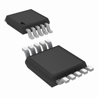
IC CTLR N-CH LOW SIDE HE 10MSOP
Manufacturer
National Semiconductor
Type
Step-Up (Boost), Flyback, Sepicr
Datasheet
1.LM3481MMNOPB.pdf
(22 pages)
Specifications of LM3481MMX/NOPB
Internal Switch(s)
No
Synchronous Rectifier
No
Number Of Outputs
1
Voltage - Output
Adjustable
Current - Output
1A
Frequency - Switching
100kHz ~ 1MHz
Voltage - Input
2.97 ~ 48 V
Operating Temperature
-40°C ~ 125°C
Mounting Type
Surface Mount
Package / Case
10-MSOP, Micro10™, 10-uMAX, 10-uSOP
For Use With
LM3481EVAL - BOARD EVAL FOR LM3481
Lead Free Status / RoHS Status
Lead free / RoHS Compliant
Power - Output
-
Other names
LM3481MMX
Available stocks
Company
Part Number
Manufacturer
Quantity
Price
Company:

Part Number:
LM3481MMX/NOPB
Manufacturer:
TI
Quantity:
12 000


V
ΔV
ΔV
V
I
V
I
V
f
V
V
R
R
V
D
t
I
I
UVLO
COMP
nom
min
SUPPLY
Q
FB
UVLOSEN
UVLOSD
COMP
sync-HI
sync-LOW
DR (max)
DS1 (ON)
DS2 (ON)
max
Symbol
Absolute Maximum Ratings
If Military/Aerospace specified devices are required,
please contact the National Semiconductor Sales Office/
Distributors for availability and specifications.
Electrical Characteristics
V
for T
min/max specification limits are guaranteed by design, test, or statistical analysis.
V
FB Pin Voltage
FA/SYNC/SD Pin Voltage
COMP Pin Voltage
UVLO Pin Voltage
V
DR Pin Voltage
I
Peak Driver Output Current
Power Dissipation
LINE
LOAD
SEN
IN
(on)
IN
CC
=12V, R
pin Voltage
J
Pin Voltage
Pin Voltage
= 25°C. Limits appearing in boldface type apply over the full Operating Temperature Range (-40°C to 125°C). Datasheet
Feedback Voltage
Feedback Voltage Line
Regulation
Output Voltage Load
Regulation
Undervoltage Lockout
Reference Voltage
UVLO Source Current
UVLO Shutdown Voltage
COMP pin Current Sink
Nominal Switching
Frequency
Threshold for
Synchronization on
FA/SYNC/SD pin
Threshold for
Synchronization on
FA/SYNC/SD pin
Driver Switch On
Resistance (top)
Driver Switch On
Resistance (bottom)
Maximum Drive Voltage
Swing(Note
Maximum Duty Cycle
Minimum On Time
Supply Current (switching)
Quiescent Current in
Shutdown Mode
FA
=40 kΩ unless otherwise indicated under the Conditions column. Typicals and limits appearing in plain type apply
Parameter
6)
V
2.97
2.97
I
V
Enabled
V
V
R
Synchronization Voltage
Rising
Synchronization Voltage
Falling
I
I
V
V
(Note
V
V
V
V
EAO
DR
DR
COMP
UVLO
FB
FB
IN
IN
FA/SYNC/SD
IN
FA/SYNC/SD
IN
FA
= 0.2A, V
= 0.2A
< 6V
≥
= 12V
= 5V
Internally Limited
= 0V
= 1.275V
–0.4V to 600 mV
= 40 kΩ
Source/Sink
≤
≤
6V
8)
Ramping Down
= 1.4V,
V
V
-0.4V to 50V
(Note
IN
IN
Conditions
-0.4V to 6V
-0.4V to 6V
-0.4V to 6V
-0.4V to 6V
-0.4V to 6V
-0.4V to 6V
≤
≤
=
=
IN
48V
48V
3V(Note
3V(Note
= 5V
1)
1.0A
9),
9),
3
Operating Ratings
Storage Temperature Range
Junction Temperature
ESD Susceptibilty
Lead Temperature
Supply Voltage
Junction Temperature Range
Switching Frequency
Range
Human Body Model
MM Package
Vapor Phase (60 sec.)
Infared (15 sec.)
1.256
1.345
Min
406
3
(Note
3,
Typical
1.275
0.003
1.430
±0.5
640
475
250
(Note
0.7
1.4
0.7
V
3.7
Note
85
5
1
4
2
6
9
5
IN
4)
2)
(Note
1.294
1.517
Max
550
5.0
15
10
6
1)
100 kHz to 1 MHz
−40°C to +125°C
−65°C to +150°C
2.97V to 48V
www.national.com
+150°C
Units
%/V
%/A
kHz
mA
215°C
220°C
µA
µA
µA
ns
%
Ω
Ω
V
V
V
V
V
V
V
2 kV
Related parts for LM3481MMX/NOPB
Image
Part Number
Description
Manufacturer
Datasheet
Request
R

Part Number:
Description:
High Efficiency Low-Side N-Channel Controller for Switching Regulators
Manufacturer:
National Semiconductor
Datasheet:

Part Number:
Description:
IC CTLR LOW SIDE N-CH SW 10MSOP
Manufacturer:
National Semiconductor
Datasheet:

Part Number:
Description:
IC, BOOST, CNTRL, 10MSOP
Manufacturer:
National Semiconductor
Datasheet:
Part Number:
Description:
National Semiconductor [8-Bit D/A Converter]
Manufacturer:
National Semiconductor
Datasheet:
Part Number:
Description:
National Semiconductor [Media Coprocessor]
Manufacturer:
National Semiconductor
Datasheet:
Part Number:
Description:
Digitally Controlled Tone and Volume Circuit with Stereo Audio Power Amplifier, Microphone Preamp Stage and National 3D Sound
Manufacturer:
National Semiconductor
Datasheet:
Part Number:
Description:
Digitally Controlled Tone and Volume Circuit with Stereo Audio Power Amplifier, Microphone Preamp Stage and National 3D Sound
Manufacturer:
National Semiconductor
Datasheet:
Part Number:
Description:
AC97 Rev 2 Codec with Sample Rate Conversion and National 3D Sound
Manufacturer:
National Semiconductor
Part Number:
Description:
Manufacturer:
National Semiconductor
Datasheet:
Part Number:
Description:
Manufacturer:
National Semiconductor
Datasheet:
Part Number:
Description:
General Purpose, Low Voltage, Low Power, Rail-to-Rail Output Operational Amplifiers
Manufacturer:
National Semiconductor
Datasheet:
Part Number:
Description:
8-bit 20 MSPS flash A/D converter.
Manufacturer:
National Semiconductor
Datasheet:
Part Number:
Description:
Low Noise Quad Operational Amplifier
Manufacturer:
National Semiconductor
Datasheet:
Part Number:
Description:
Quad Differential Line Receivers
Manufacturer:
National Semiconductor
Datasheet: