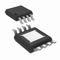
LM5085MY/NOPB National Semiconductor, LM5085MY/NOPB Datasheet - Page 4

LM5085MY/NOPB
Manufacturer Part Number
LM5085MY/NOPB
Description
IC BUCK ADJ 8MSOPEP
Manufacturer
National Semiconductor
Series
PowerWise®r
Type
Step-Down (Buck)r
Datasheet
1.LM5085MYENOPB.pdf
(22 pages)
Specifications of LM5085MY/NOPB
Design Resources
LM(2)5085 Quick Start Calculator
Internal Switch(s)
No
Synchronous Rectifier
No
Number Of Outputs
1
Voltage - Output
1.25 ~ 75 V
Frequency - Switching
Up to 1MHz
Voltage - Input
4.5 ~ 75 V
Operating Temperature
-40°C ~ 125°C
Mounting Type
Surface Mount
Package / Case
8-MSOP Exposed Pad, 8-HMSOP, 8-eMSOP
Lead Free Status / RoHS Status
Lead free / RoHS Compliant
Current - Output
-
Power - Output
-
Other names
LM5085MY
Available stocks
Company
Part Number
Manufacturer
Quantity
Price
Company:
Part Number:
LM5085MY/NOPB
Manufacturer:
TI
Quantity:
1 001
Part Number:
LM5085MY/NOPB
Manufacturer:
TI/德州仪器
Quantity:
20 000
www.national.com
VIN Pin
VCC Regulator (Note 3)
PGATE Pin
Current Limit Detection
RT Pin
On-Time
VIN to GND
ISEN to GND
ADJ to GND
RT, FB to GND
V
Absolute Maximum Ratings
If Military/Aerospace specified devices are required,
please contact the National Semiconductor Sales Office/
Distributors for availability and specifications.
Electrical Characteristics
junction temperature (T
correlation. Typical values represent the most likely parametric norm at T
Unless otherwise stated the following conditions apply: VIN = 48V, R
V
V
V
V
PGATE(LO)4.5
UVLO
PGATE(HI)4.5
Symbol
V
PGATE(LO)
R
CL OFFSET
V
PGATE(HI)
RT
I
t
t
RT
t
t
PGATE
ON – 1
ON – 2
CC(reg)
ON - 3
ON - 4
CC(CL)
PGATE
I
I
ADJ
I
IN
Q
HYS
SD
Vcc
Parameter
Operating current
Shutdown current
VIN - VCC
VCC under-voltage lock-out threshold
UVLO
VCC Current Limit
PGATE High voltage
PGATE Low voltage
PGATE High Voltage at Vin = 4.5V
PGATE Low Voltage at Vin = 4.5V
Driver Output Source Current
Driver Output Sink Current
Driver Output Resistance
ADJUST pin current source
Current limit comparator offset
Shutdown threshold
Shutdown threshold hysteresis
On-time
Minimum on-time in current limit
Vcc
J
) range of -40°C to +125°C. Minimum and Maximum limits are guaranteed through test, design, or statistical
hysteresis
-0.3V to 76V
-0.3V to V
-0.3V to V
-0.3V to 7V
Limits in standard type are for T
(Note
(Note
IN
IN
+ 0.3V
+ 0.3V
1)
7) VIN = 48V, 25 mV overdrive at ISEN
Conditions
Non-switching, FB = 1.4V
RT = 0V
Vin = 9V, FB = 1.4V, ICC = 0 mA
Vin = 9V, FB = 1.4V, ICC = 20 mA
Vin = 75V, FB = 1.4V, ICC = 0 mA
V
V
FB = 1.4V
PGATE Pin = Open
PGATE Pin = Open
PGATE Pin = Open
PGATE Pin = Open
VIN = 12V, PGATE = VIN - 3.5V
VIN = 12V, PGATE = VIN - 3.5V
Source current = 500 mA
Sink current = 500 mA
V
V
RT Pin voltage rising
VIN = 4.5V, R
VIN = 48V, R
VIN = 75V, R
CC
CC
ADJ
ADJ
increasing
decreasing
4
= 46.5V
= 46.5V, V
VIN to VCC, VIN to PGATE
ESD Rating
Storage Temperature Range
VIN Voltage
Junction Temperature
(Note
Operating Ratings
T
Human Body Model
= 100 kΩ.
T
T
J
T
= 100 kΩ
= 100 kΩ
6)
= 25°C, and are provided for reference purposes only.
= 100 kΩ
ADJ
J
= 25°C only; limits in boldface type apply over the
- V
(Note
ISEN
(Note
2)
6)
V
V
IN
IN
Min
276
177
6.9
3.5
20
32
55
-9
(Note
-0.1
-0.1
1)
1.75
0.73
-0.3V to 10V
2kV
-65°C to +150°C
Typ
200
260
V
V
360
235
140
1.3
7.7
7.7
7.7
3.8
V
V
1.5
2.3
2.3
40
40
50
0
5
CC
CC
−40°C to + 125°C
IN
IN
4.5V to 75V
Max
+0.1
+0.1
7.15
345
V
V
435
285
235
1.8
8.5
48
9
CC
CC
Units
mA
mV
mA
mV
mV
µA
µA
µs
ns
ns
ns
V
V
V
V
V
V
V
V
A
A
Ω
Ω
V


