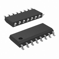
LM3524DMX/NOPB National Semiconductor, LM3524DMX/NOPB Datasheet - Page 8

LM3524DMX/NOPB
Manufacturer Part Number
LM3524DMX/NOPB
Description
IC REG PULSE WIDTH MOD 16-SOIC
Manufacturer
National Semiconductor
Type
Step-Down (Buck), Step-Up (Boost), Flybackr
Datasheet
1.LM2524DNNOPB.pdf
(22 pages)
Specifications of LM3524DMX/NOPB
Internal Switch(s)
Yes
Synchronous Rectifier
No
Number Of Outputs
1
Voltage - Output
5V
Current - Output
200mA
Frequency - Switching
550kHz
Voltage - Input
8 ~ 40 V
Operating Temperature
0°C ~ 125°C
Mounting Type
Surface Mount
Package / Case
16-SOIC (3.9mm Width)
Power - Output
1W
Number Of Pwm Outputs
2
On/off Pin
Yes
Adjustable Output
Yes
Switching Freq
350KHz
Duty Cycle
49%
Operating Supply Voltage (max)
40V
Output Current
200A
Output Voltage
60V
Synchronous Pin
Yes
Rise Time
200ns
Fall Time
100ns
Operating Temperature Classification
Commercial
Mounting
Surface Mount
Pin Count
16
Package Type
SOIC N
Lead Free Status / RoHS Status
Lead free / RoHS Compliant
Other names
*LM3524DMX
*LM3524DMX/NOPB
LM3524DMX
*LM3524DMX/NOPB
LM3524DMX
www.national.com
Functional Description
INTERNAL VOLTAGE REGULATOR
The LM3524D has an on-chip 5V, 50 mA, short circuit pro-
tected voltage regulator. This voltage regulator provides a
supply for all internal circuitry of the device and can be used
as an external reference.
For input voltages of less than 8V the 5V output should be
shorted to pin 15, V
these pins shorted the input voltage must be limited to a max-
imum of 6V. If input voltages of 6V–8V are to be used, a pre-
regulator, as shown in Figure 1, must be added.
*Minimum C
OSCILLATOR
The LM3524D provides a stable on-board oscillator. Its fre-
quency is set by an external resistor, R
graph of R
The oscillator's output provides the signals for triggering an
internal flip-flop, which directs the PWM information to the
outputs, and a blanking pulse to turn off both outputs during
transitions to ensure that cross conduction does not occur.
The width of the blanking pulse, or dead time, is controlled by
the value of C
values of R
μF.
If two or more LM3524D's must be synchronized together, the
easiest method is to interconnect all pin 3 terminals, tie all pin
7's (together) to a single C
one which is connected to a single R
unless the LM3524D's are more than 6 apart.
A second synchronization method is appropriate for any cir-
cuit layout. One LM3524D, designated as master, must have
its R
(s) should each have an R
pin 3's must then be interconnected to allow the master to
properly reset the slave units.
The oscillator may be synchronized to an external clock
source by setting the internal free-running oscillator frequen-
cy 10% slower than the external clock and driving pin 3 with
a pulse train (approx. 3V) from the clock. Pulse width should
be greater than 50 ns to insure full synchronization.
T
C
T
set for the correct period. The other slave LM3524D
O
T
T
of 10 μF required for stability.
, C
are 1.8 kΩ to 100 kΩ, and for C
T
T
, as shown in Figure 3. The recommended
vs oscillator frequency is shown is Figure 2.
IN
, which disables the 5V regulator. With
FIGURE 1.
T
T
C
, and leave all pin 6's open except
T
set for a 10% longer period. All
T
. This method works well
T
and capacitor, C
T
, 0.001 μF to 0.1
865010
T
. A
8
ERROR AMPLIFIER
The error amplifier is a differential input, transconductance
amplifier. Its gain, nominally 86 dB, is set by either feedback
or output loading. This output loading can be done with either
purely resistive or a combination of resistive and reactive
components. A graph of the amplifier's gain vs output load
resistance is shown in Figure 4.
FIGURE 2.
FIGURE 3.
FIGURE 4.
865005
865006
865007


