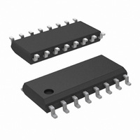
LM3524DMX/NOPB National Semiconductor, LM3524DMX/NOPB Datasheet - Page 17

LM3524DMX/NOPB
Manufacturer Part Number
LM3524DMX/NOPB
Description
IC REG PULSE WIDTH MOD 16-SOIC
Manufacturer
National Semiconductor
Type
Step-Down (Buck), Step-Up (Boost), Flybackr
Datasheet
1.LM2524DNNOPB.pdf
(22 pages)
Specifications of LM3524DMX/NOPB
Internal Switch(s)
Yes
Synchronous Rectifier
No
Number Of Outputs
1
Voltage - Output
5V
Current - Output
200mA
Frequency - Switching
550kHz
Voltage - Input
8 ~ 40 V
Operating Temperature
0°C ~ 125°C
Mounting Type
Surface Mount
Package / Case
16-SOIC (3.9mm Width)
Power - Output
1W
Number Of Pwm Outputs
2
On/off Pin
Yes
Adjustable Output
Yes
Switching Freq
350KHz
Duty Cycle
49%
Operating Supply Voltage (max)
40V
Output Current
200A
Output Voltage
60V
Synchronous Pin
Yes
Rise Time
200ns
Fall Time
100ns
Operating Temperature Classification
Commercial
Mounting
Surface Mount
Pin Count
16
Package Type
SOIC N
Lead Free Status / RoHS Status
Lead free / RoHS Compliant
Other names
*LM3524DMX
*LM3524DMX/NOPB
LM3524DMX
*LM3524DMX/NOPB
LM3524DMX
THE STEP-UP SWITCHING REGULATOR
Figure 18 shows the basic circuit for a step-up switching reg-
ulator. In this circuit Q1 is used as a switch to alternately apply
V
energy is drawn from V
ased and I
Q1 opens, t
where D1 turns ON. The output current is now supplied
through L1, D1 to the load and any charge lost from C
t
the current through L1 has a DC component plus some ΔI
ΔI
19 shows the inductor's current in relation to Q1's ON and
OFF times.
Since ΔI
and neglecting V
The above equation shows the relationship between V
and duty cycle.
In calculating input current I
DC current, assume first 100% efficiency:
for η = 100%, P
ON
IN
L
is replenished. Here also, as in the step-down regulator,
across inductor L1. During the time, t
is again selected to be approximately 40% of I
L
+ = ΔI
o
OFF
is supplied from the charge stored in C
L
, voltage V1 will rise positively to the point
OUT
−, V
SAT
= P
IN
and V
FIGURE 19. Relation of Switch Timing to Inductor Current in Step-Up Regulator
t
ON
IN
IN
and stored in L1; D1 is reverse bi-
= V
D1
IN(DC)
o
t
OFF
, which equals the inductor's
− V
IN
t
OFF
ON
,
, Q1 is ON and
L
o
. Figure
o
. When
during
IN
, V
L
o
.
17
This equation shows that the input, or inductor, current is
larger than the output current by the factor (1 + t
this factor is the same as the relation between V
(DC)
So far it is assumed η = 100%, where the actual efficiency or
η
Q1 and forward on voltage of D1. The internal power loss due
to these voltages is the average I
through either V
loss becomes I
This equation assumes only DC losses, however η
ther decreased because of the switching time of Q1 and D1.
MAX
can also be expressed as:
FIGURE 18. Basic Step-Up Switching Regulator
will be somewhat less due to the saturation voltage of
IN(DC)
SAT
or V
(1V). η
D1
. For V
MAX
is then:
865024
SAT
L
current flowing, or I
= V
D1
= 1V this power
ON
o
/t
www.national.com
and V
OFF
MAX
). Since
865023
is fur-
IN
, I
IN
IN
,


