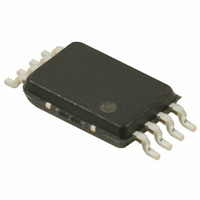
S-8341A30AFT-T2-G Seiko Instruments, S-8341A30AFT-T2-G Datasheet - Page 23

S-8341A30AFT-T2-G
Manufacturer Part Number
S-8341A30AFT-T2-G
Description
IC REG SW 600KHZ 3.0V 8-TSSOP
Manufacturer
Seiko Instruments
Type
Step-Up (Boost)r
Datasheet
1.S-8340A25AFT-T2-G.pdf
(55 pages)
Specifications of S-8341A30AFT-T2-G
Internal Switch(s)
No
Synchronous Rectifier
No
Number Of Outputs
1
Voltage - Output
3V
Frequency - Switching
600kHz
Voltage - Input
0.9 ~ 6 V
Operating Temperature
-40°C ~ 85°C
Mounting Type
Surface Mount
Package / Case
8-TSSOP
Power - Output
300mW
Output Voltage
3 V
Operating Temperature Range
- 40 C to + 85 C
Mounting Style
SMD/SMT
Lead Free Status / RoHS Status
Lead free / RoHS Compliant
Current - Output
-
Lead Free Status / Rohs Status
Lead free / RoHS Compliant
STEP-UP, 600 kHz, PWM CONTROL OR PWM/PFM SWITCHABLE SWITCHING REGULATOR CONTROLLER
Rev.4.0
5. External Transistors
5. 1 Enhancement (N-Channel) MOS FET Type
5. 2 Bipolar (NPN) Type
Enhancement (N-channel) MOS FET type or bipolar (NPN) type can be used for the external transistors.
The EXT pin can directly drive an N-channel MOS FET. When an N-channel MOS FET is used, efficiency will be 2
to 3% higher than that achieved by an NPN bipolar transistor since the MOS FET switching speed is faster and
power dissipation due to the base current is avoided.
A large current may flow at power on with some MOS FETs selected. Perform thorough evaluation using the actual
devices to select. The recommended gate capacitance of the MOS FET to be used is 1200 pF or smaller.
The important parameters in selecting a MOS FET are threshold voltage, breakdown voltage between drain and
source, total gate capacitance, on-resistance, and the current rating.
The EXT pin voltage swings between V
enough so that the MOS FET is completely turned on must be used. If V
the gate and source must be higher by at least several volts.
During the step-up operation, voltage V
breakdown voltage between the drain and source should be higher than the V
volts.
The total gate capacitance and the on-resistance affect the efficiency.
The larger the total gate capacitance becomes and the higher the input voltage becomes, the more the power
dissipation for charging and discharging the gate capacitance by switching operation increases, and affects the
efficiency at low load current region. If the efficiency at low load is important, select MOS FETs with a small total
gate capacitance.
In the regions where the load current is high, the efficiency is affected by power dissipation caused by the
resistance of the MOS FETs. If the efficiency under heavy load is particularly important in the application, choose
MOS FETs which have an on-resistance as low as possible. As for the current rating, select a MOS FET whose
maximum continuous drain current rating is higher than I
Figures 16 and 17 in “
Sanyo Electric Co., Ltd. 2SD1628G for the bipolar transistor (NPN). The driveability for increasing the output
current by means of a bipolar transistor depend on the h
The R
Find the necessary base current (I
select a smaller R
A small R
voltage drops take place due to the wiring resistance or some other reason. Determine an optimum value through
experimentation.
In addition, if a speed-up capacitor (C
17, the switching loss will be reduced, leading to a higher efficiency.
Select a C
However, the optimum C
value after performing a thorough evaluation.
_00
R
C
b
b
b
=
≤
value is given by the following equation :
b
V
2
b
DD
value can increase the output current, but the efficiency decreases. A current may flow as the pulses or
π ×
value by using the following equation as a guide :
− 0.7
I
b
R
b
b
×
value.
1
fosc
−
I
EXTH
0.4
b
Standard Circuits (2) Using Bipolar Transistors” show sample circuit diagrams using
×
value differs depending upon the characteristics of the bipolar transistor. Select a C
0.1
b
) using the h
b
) is inserted in parallel with the resistance (R
DD
OUT
and V
+ V
Seiko Instruments Inc.
F
SS
is applied between the drain and source of the MOS FET. So the
FE
. If V
v alue of the bipolar transistor by the equation, I
FE
DD
PK
.
and R
is low, a MOS FET of which the threshold voltage is low
b
values of that bipolar transistor.
DD
is high, the breakdown voltage between
OUT
+ V
b
) as shown in Figures 16 and
S-8340/8341 Series
F
voltage by at least several
b
= I
PK
/h
FE
, and
23
b


