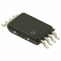
S-8341A30AFT-T2-G Seiko Instruments, S-8341A30AFT-T2-G Datasheet - Page 20

S-8341A30AFT-T2-G
Manufacturer Part Number
S-8341A30AFT-T2-G
Description
IC REG SW 600KHZ 3.0V 8-TSSOP
Manufacturer
Seiko Instruments
Type
Step-Up (Boost)r
Datasheet
1.S-8340A25AFT-T2-G.pdf
(55 pages)
Specifications of S-8341A30AFT-T2-G
Internal Switch(s)
No
Synchronous Rectifier
No
Number Of Outputs
1
Voltage - Output
3V
Frequency - Switching
600kHz
Voltage - Input
0.9 ~ 6 V
Operating Temperature
-40°C ~ 85°C
Mounting Type
Surface Mount
Package / Case
8-TSSOP
Power - Output
300mW
Output Voltage
3 V
Operating Temperature Range
- 40 C to + 85 C
Mounting Style
SMD/SMT
Lead Free Status / RoHS Status
Lead free / RoHS Compliant
Current - Output
-
Lead Free Status / Rohs Status
Lead free / RoHS Compliant
20
STEP-UP, 600 kHz, PWM CONTROL OR PWM/PFM SWITCHABLE SWITCHING REGULATOR CONTROLLER
S-8340/8341 Series
1. Method for Selecting Series Products
Series Products and External Parts Selection
1. 1 Control Systems
1. 2 Oscillation Frequencies
1. 3 Output Voltage Setting
The S-8340/8341 Series is classified into eight types, according to the control systems (PWM and PWM/PFM
switching), oscillation frequencies, and output voltage setting types.
The following describes the features of respective types. Select the type according to the applications.
Two different control systems are available : PWM control system (S-8340 Series) and PWM/PFM switching control
system (S-8341 Series).
For applications for which the load current greatly differs between standby and operation, if the efficiency during
standby is important, applying the PWM/PFM switching system (S-8341 Series) realizes high efficiency during
standby.
For applications for which switching noise is critical, applying the PWM control system (S-8340 Series) whereby
switching frequency does not change due to load current allows the ripple voltage to be easily eliminated by using a
filter.
Either oscillation frequencies, 600 kHz (A and B types) or 300 kHz (C and D types), can be selected.
The A and B types whereby high operation frequency allows the L value to be reduced, so a small inductor can be
used. In addition, use of small output capacitors is effective for downsizing devices.
The C and D types, whereby lower oscillation frequency realizes smaller self-consumption current, are highly
efficient under light loads. In particular, the C type, when combined with a PWM/PFM switching control system,
drastically improves the operation efficiency when the output load current is approximately 1 mA.
Either fixed output type (A and C types) or external setting type (B and D types) can be selected.
The A and C types, whereby output voltage can be internally set between 2.5 and 6.0 V in the 0.1 V steps, realizes
highly accurate output voltage of ±2.0% with internal highly resistant and highly accurate resistors.
In the B and D types, the output voltage can be adjusted in the range 2.5 to 6.0 V by adding external resistors (R
and R
A temperature gradient can be provided by installing a thermistor in series to R
The resistance of R
Add C
Set C
Example : V
The accuracy of the output voltage V
external resistors R
precision of the voltage at FB pin (1 V ±2.0%).
When it is assumed that I
R
R
(V
FB1
FB2
OUT
max. and R
min., and the shift of the output voltage due to the dependence of voltage on V
FB
FB2
min.) and maximum value (V
FB
so that f
) and a capacitor (C
in parallel with R
OUT
= 3.0 V, R
FB2
OSC
max., the minimum absolute value variations of external resistors R
FB1
FB1
= 1/(2 × π × C
+ R
and R
FB1
FB
FB1
FB2
FB
is 0 nA, the maximum absolute value variations of external resistors R
to prevent unstable operation due to output oscillation.
= 200 kΩ, R
FB2
must not exceed 2 MΩ, and set the ratio of R
).
, the FB pin input current (I
FB
OUT
× R
OUT
max.) of variations of V
FB1
FB2
set with resistors R
) is 0.1 to 20 kHz (normally, 10 kHz).
Seiko Instruments Inc.
= 100 kΩ, C
FB
= 100 pF
FB
OUT
FB1
) and IC power supply voltage (V
are expressed by the following formulas :
and R
FB2
FB1
is affected by the absolute precision of
FB1
to R
and R
FB2
FB1
so that the FB pin is at 1.0 V.
DD
FB2
and R
is ΔV, the minimum value
.
FB2
DD
are R
FB1
) as well as the
Rev.4.0
and R
FB1
min. and
FB2
_00
are
FB1


