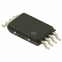
S-8340A30AFT-T2-G Seiko Instruments, S-8340A30AFT-T2-G Datasheet - Page 21

S-8340A30AFT-T2-G
Manufacturer Part Number
S-8340A30AFT-T2-G
Description
IC REG SW 600KHZ 3.0V 8-TSSOP
Manufacturer
Seiko Instruments
Type
Step-Up (Boost)r
Datasheet
1.S-8340A25AFT-T2-G.pdf
(55 pages)
Specifications of S-8340A30AFT-T2-G
Internal Switch(s)
No
Synchronous Rectifier
No
Number Of Outputs
1
Voltage - Output
3V
Frequency - Switching
600kHz
Voltage - Input
0.9 ~ 6 V
Operating Temperature
-40°C ~ 85°C
Mounting Type
Surface Mount
Package / Case
8-TSSOP
Power - Output
300mW
Output Voltage
3 V
Operating Temperature Range
- 40 C to + 85 C
Mounting Style
SMD/SMT
Lead Free Status / RoHS Status
Lead free / RoHS Compliant
Current - Output
-
Lead Free Status / Rohs Status
Lead free / RoHS Compliant
STEP-UP, 600 kHz, PWM CONTROL OR PWM/PFM SWITCHABLE SWITCHING REGULATOR CONTROLLER
Rev.4.0
R
±2.0%) or lower. The smaller R
and R
To reduce the influence due to I
lower than the input impedance at the FB pin (1 V/50 nA = 20 MΩ (max.)).
Reactive current flows through R
respect to the actual load current, efficiency decreases. Therefore, R
Caution If the R
Since the accuracy of V
application requirements.
Caution Connect the VDD pin to the VOUT pin for both the fixed output types and external setting types
The table below provides a rough guide for selecting a product type according to the application requirements of the
application.
Choose the product that gives you the largest number of circles (O).
FB1
_00
Remark
The set output voltage is 6 V or less
Set an output voltage freely
The efficiency under light loads (approx. 1mA) is an
important factor
To be operated with a medium load current (200 mA
class)
To be operated with a high load current (1 A class)
It is important to have a low-ripple voltage
Downsizing of external components is important
and R
FB2
. The smaller R
noise, therefore, thoroughly test the performance with the actual equipment.
as shown in “
power source instead of V
B types, 6.0 ms: C and D types).
When the VDD pin is connected to the VOUT pin, V
problems.
FB2
The symbol "
corresponding series has superiority in that aspect. The symbol " " indicates particularly high
superiority.
V
V
must be adjusted in order to set the voltage accuracy of V
OUT
OUT
FB1
min. = (1+
max. = (1+
and R
FB1
OUT
Standard Circuit”. In the cases when V
and R
FB2
and reactive current must be traded off, they must be considered according to
" denotes an indispensable condition, while the symbol " " indicates that the
R
R
R
R
values are too large (1 MΩ or more), V
FB
FB1
FB2
FB1
FB1
FB2
FB1
FB2
that affects variations of V
max.
max.
and R
min.
min.
and R
are, the less V
OUT
, raise V
FB2
) × 0.98 − ΔV [V]
) × 102 + ΔV [V]
FB2
Seiko Instruments Inc.
are, the less V
. Unless the reactive current value is limited as low as possible with
Table 9
DD
OUT
to 2.5 V or higher within the soft-start time (3.0 ms: A and
is affected by I
A
OUT
OUT
B
is affected by the absolute value accuracy of R
, the R
S-8340
FB1
FB
DD
IN
C
FB2
.
OUT
and R
OUT
requires to be applied from V
can be increased slowly without any
value must be set to a value sufficiently
to the IC output voltage accuracy (V
is subject to be affected by external
FB2
D
should be sufficiently large.
A
S-8340/8341 Series
B
S-8341
C
IN
or other
D
OUT
FB1
21


