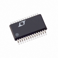
LTC3890EGN-1#PBF Linear Technology, LTC3890EGN-1#PBF Datasheet - Page 18

LTC3890EGN-1#PBF
Manufacturer Part Number
LTC3890EGN-1#PBF
Description
IC BUCK SYNC ADJ 25A DUAL 28SSOP
Manufacturer
Linear Technology
Type
Step-Down (Buck)r
Specifications of LTC3890EGN-1#PBF
Internal Switch(s)
No
Synchronous Rectifier
Yes
Number Of Outputs
2
Voltage - Output
0.8 ~ 24 V
Current - Output
25A
Frequency - Switching
50kHz ~ 900kHz
Voltage - Input
4 ~ 60 V
Operating Temperature
-40°C ~ 125°C
Mounting Type
Surface Mount
Package / Case
28-SSOP
Primary Input Voltage
12V
No. Of Outputs
2
Output Voltage
24V
Output Current
25A
No. Of Pins
32
Operating Temperature Range
-40°C To +125°C
Msl
MSL 1 - Unlimited
Supply Voltage Min
4V
Rohs Compliant
Yes
Lead Free Status / RoHS Status
Lead free / RoHS Compliant
Power - Output
-
LTC3890
The peak-to-peak drive levels are set by the INTV
This voltage is typically 5.1V during start-up (see EXTV
Pin Connection). Consequently, logic-level threshold
MOSFETs must be used in most applications. Pay close
attention to the BV
Selection criteria for the power MOSFETs include the
on-resistance, R
voltage and maximum output current. Miller capacitance,
C
usually provided on the MOSFET manufacturers’ data
sheet. C
along the horizontal axis while the curve is approximately
flat divided by the specified change in V
then multiplied by the ratio of the application applied V
to the gate charge curve specified V
operating in continuous mode the duty cycles for the top
and bottom MOSFETs are given by:
The MOSFET power dissipations at maximum output
current are given by:
APPLICATIONS INFORMATION
18
MILLER
Main Switch Duty Cycle =
P
P
Synchronous Switch Duty Cycle =
SYNC
MAIN
, can be approximated from the gate charge curve
MILLER
=
=
⎡
⎢
⎣
( )
V
V
V
V
V
OUT
IN
IN
INTVCC
IN
– V
is equal to the increase in gate charge
V
DS(ON)
2
DSS
IN
(
⎛
⎜
⎝
I
OUT
MAX
I
MAX
specification for the MOSFETs as well.
1
– V
2
, Miller capacitance, C
)
(
I
2
THMIN
⎞
⎟ R
⎠
MAX
(
(
1+ δ
DR
)
2
V
)
+
)
(
V
OUT
(
R
1+ δ
C
IN
V
DS(ON)
MILLER
THMIN
1
)
DS
R
. When the IC is
V
DS(ON)
DS
IN
+
⎤
⎥ f
⎦
)
( )
. This result is
•
− V
V
MILLER
IN
CC
OUT
voltage.
, input
CC
DS
where δ is the temperature dependency of R
R
at the MOSFET’s Miller threshold voltage. V
typical MOSFET minimum threshold voltage.
Both MOSFETs have I
equation includes an additional term for transition losses,
which are highest at high input voltages. For V
the high current efficiency generally improves with larger
MOSFETs, while for V
increase to the point that the use of a higher R
with lower C
synchronous MOSFET losses are greatest at high input
voltage when the top switch duty factor is low or during
a short-circuit when the synchronous switch is on close
to 100% of the period.
The term (1+ δ) is generally given for a MOSFET in the
form of a normalized R
δ = 0.005/°C can be used as an approximation for low
voltage MOSFETs.
The optional Schottky diodes D3 and D4 shown in
Figure 11 conduct during the dead-time between the
conduction of the two power MOSFETs. This prevents
the body diode of the bottom MOSFET from turning on,
storing charge during the dead-time and requiring a
reverse recovery period that could cost as much as 3%
in efficiency at high V
a good compromise for both regions of operation due
to the relatively small average current. Larger diodes
result in additional transition losses due to their larger
junction capacitance.
C
The selection of C
ture and its impact on the worst-case RMS current drawn
through the input network (battery/fuse/capacitor). It can be
shown that the worst-case capacitor RMS current occurs
when only one controller is operating. The controller with
the highest (V
formula shown in Equation 1 to determine the maximum
IN
DR
and C
(approximately 2Ω) is the effective driver resistance
OUT
MILLER
Selection
OUT
)(I
IN
actually provides higher efficiency. The
is simplified by the 2-phase architec-
OUT
2
IN
R losses while the topside N-channel
IN
DS(ON)
> 20V the transition losses rapidly
. A 1A to 3A Schottky is generally
) product needs to be used in the
vs Temperature curve, but
DS(ON)
THMIN
DS(ON)
IN
device
< 20V
is the
3890fa
and


