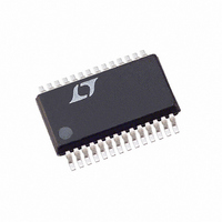
LTC3890EGN-1#PBF Linear Technology, LTC3890EGN-1#PBF Datasheet - Page 17

LTC3890EGN-1#PBF
Manufacturer Part Number
LTC3890EGN-1#PBF
Description
IC BUCK SYNC ADJ 25A DUAL 28SSOP
Manufacturer
Linear Technology
Type
Step-Down (Buck)r
Specifications of LTC3890EGN-1#PBF
Internal Switch(s)
No
Synchronous Rectifier
Yes
Number Of Outputs
2
Voltage - Output
0.8 ~ 24 V
Current - Output
25A
Frequency - Switching
50kHz ~ 900kHz
Voltage - Input
4 ~ 60 V
Operating Temperature
-40°C ~ 125°C
Mounting Type
Surface Mount
Package / Case
28-SSOP
Primary Input Voltage
12V
No. Of Outputs
2
Output Voltage
24V
Output Current
25A
No. Of Pins
32
Operating Temperature Range
-40°C To +125°C
Msl
MSL 1 - Unlimited
Supply Voltage Min
4V
Rohs Compliant
Yes
Lead Free Status / RoHS Status
Lead free / RoHS Compliant
Power - Output
-
The equivalent resistance R1|| R2 is scaled to the room
temperature inductance and maximum DCR:
The sense resistor values are:
The maximum power loss in R1 is related to duty cycle,
and will occur in continuous mode at the maximum input
voltage:
Ensure that R1 has a power rating higher than this value.
If high efficiency is necessary at light loads, consider this
power loss when deciding whether to use DCR sensing or
sense resistors. Light load power loss can be modestly
higher with a DCR network than with a sense resistor, due
to the extra switching losses incurred through R1. However,
DCR sensing eliminates a sense resistor, reduces conduc-
tion losses and provides higher efficiency at heavy loads.
Peak efficiency is about the same with either method.
Inductor Value Calculation
The operating frequency and inductor selection are inter-
related in that higher operating frequencies allow the use
of smaller inductor and capacitor values. So why would
anyone ever choose to operate at lower frequencies with
larger components? The answer is efficiency. A higher
frequency generally results in lower efficiency because of
MOSFET switching and gate charge losses. In addition to
this basic trade-off, the effect of inductor value on ripple
current and low current operation must also be considered.
The inductor value has a direct effect on ripple current. The
inductor ripple current, ΔI
tance or higher frequency and increases with higher V
APPLICATIONS INFORMATION
R1|| R2 =
R1=
P
ΔI
LOSS
L
=
R1|| R2
( )
R1=
R
f
D
1
( )
(
L
DCR at 20°C
(
; R2 =
V
V
IN(MAX)
OUT
⎛
⎜
⎝
L
1–
R1• R
1– R
– V
L
V
R1
, decreases with higher induc-
)
V
OUT
D
OUT
• C1
D
IN
⎞
⎟
⎠
)
• V
OUT
IN
:
Accepting larger values of ΔI
inductances, but results in higher output voltage ripple
and greater core losses. A reasonable starting point for
setting ripple current is ΔI
ΔI
The inductor value also has secondary effects. The tran-
sition to Burst Mode operation begins when the average
inductor current required results in a peak current below
25% of the current limit determined by R
inductor values (higher ΔI
lower load currents, which can cause a dip in efficiency in
the upper range of low current operation. In Burst Mode
operation, lower inductance values will cause the burst
frequency to decrease.
Inductor Core Selection
Once the value for L is known, the type of inductor must
be selected. High efficiency converters generally cannot
afford the core loss found in low cost powdered iron cores,
forcing the use of more expensive ferrite or molypermalloy
cores. Actual core loss is independent of core size for a
fixed inductor value, but it is very dependent on inductance
value selected. As inductance increases, core losses go
down. Unfortunately, increased inductance requires more
turns of wire and therefore copper losses will increase.
Ferrite designs have very low core loss and are preferred
for high switching frequencies, so design goals can con-
centrate on copper loss and preventing saturation. Ferrite
core material saturates hard, which means that induc-
tance collapses abruptly when the peak design current is
exceeded. This results in an abrupt increase in inductor
ripple current and consequent output voltage ripple. Do
not allow the core to saturate!
Power MOSFET and Schottky Diode
(Optional) Selection
Two external power MOSFETs must be selected for each
controller in the LTC3890: one N-channel MOSFET for the
top (main) switch, and one N-channel MOSFET for the
bottom (synchronous) switch.
L
occurs at the maximum input voltage.
L
L
) will cause this to occur at
= 0.3(I
L
allows the use of low
MAX
LTC3890
). The maximum
SENSE
. Lower
17
3890fa


