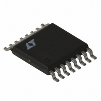
LT3434IFE#PBF Linear Technology, LT3434IFE#PBF Datasheet

LT3434IFE#PBF
Specifications of LT3434IFE#PBF
Available stocks
Related parts for LT3434IFE#PBF
LT3434IFE#PBF Summary of contents
Page 1
... Distributed Power Systems ■ Battery-Powered Systems , LTC and LT are registered trademarks of Linear Technology Corporation. All other trademarks are the property of their respective owners. Burst Mode is a registered trademark of Linear Technology Corporation. *Protected by U.S. Patents including 6498466. **See Burst Mode Operation section for conditions. ...
Page 2
LT3434 ABSOLUTE AXI U RATI GS (Note SHDN, BIAS, PGOOD, SW ............................... 60V IN BOOST Pin Above SW ............................................ 35V BOOST Pin Voltage ................................................. 68V SYNC PGFB, FB ................................................ 6V SS Operating ...
Page 3
ELECTRICAL CHARACTERISTICS temperature range, otherwise specifications are /SYNC = 0V unless otherwise noted. SS SYMBOL PARAMETER V High Clamp Current Limit PK Switch On Resistance (Note 9) Switching Frequency Maximum Duty Cycle Minimum SYNC ...
Page 4
LT3434 W U TYPICAL PERFOR A CE CHARACTERISTICS FB Voltage 1.30 1.29 1.28 1.27 1.26 1.25 1.24 1.23 1.22 1.21 1.20 –50 – 100 125 TEMPERATURE (°C) 3434 G01 SHDN Pin Current 5 25°C ...
Page 5
W U TYPICAL PERFOR A CE CHARACTERISTICS Switch Peak Current Limit 6.0 5.5 5.0 4.5 4.0 3.5 3.0 –50 –25 – 100 125 TEMPERATURE (°C) 3434 G10 Switch On Voltage (V ) CESAT 500 450 400 T ...
Page 6
LT3434 W U TYPICAL PERFOR A CE CHARACTERISTICS 3.3V Dropout Operation 4 3.3V OUT BOOST DIODE = DIODES INC B1100 3.5 3.0 2.5 LOAD CURRENT 2.0 0.25A LOAD CURRENT 1.5 2.5A 1.0 0 0.5 1 1.5 ...
Page 7
CTIO S from the C pin into the external capacitor. When the volt- T age on the external capacitor reaches an internal clamp (V ), the PG pin becomes a high impedance node. The CT ...
Page 8
LT3434 W BLOCK DIAGRA INTERNAL REF 4 UNDERVOLTAGE LOCKOUT BIAS THERMAL 10 SHUTDOWN SYNC 14 SHDN + 15 SHDN COMP – 1. SOFT-START FOLDBACK DETECT FB – 12 ERROR AMP + 1.25V ...
Page 9
W BLOCK DIAGRA power from the V pin, but if the BIAS pin is connected external voltage higher than 3V bias power will be drawn from the external source (typically the regulated output voltage). This improves efficiency. ...
Page 10
LT3434 U U APPLICATIO S I FOR ATIO and Soft-Start Current graphs in Typical Performance Characteristics). Frequency foldback is done to control power dissipation in both the IC and in the external diode and inductor during short-circuit conditions. A shorted ...
Page 11
U U APPLICATIO S I FOR ATIO taken to ensure the ripple and surge ratings are not exceeded. The AVX TPS and Kemet T495 series are surge rated AVX recommends derating capacitor operating volt- age by 2:1 for high surge ...
Page 12
LT3434 U U APPLICATIO S I FOR ATIO V OUT 10mV/DIV 100µF 75mΩ TANTALUM V OUT 10mV/DIV 100µF CERAMIC I SW 10V/DIV 1µs/DIV LOAD Figure 3. LT3434 Ripple Voltage Waveform For high frequency switchers the ripple current ...
Page 13
U U APPLICATIO S I FOR ATIO To calculate actual peak switch current in continuous mode with a given set of conditions, use – V OUT IN OUT = + ( )( )( ) ...
Page 14
... After making an initial choice, consider the secondary things like output voltage ripple, second sourcing, etc. Use the experts in the Linear Technology’s applications department if you feel uncertain about the final choice. They have experience with a wide range of inductor types and can tell you about the latest developments in low profile, surface mounting, etc ...
Page 15
U U APPLICATIO S I FOR ATIO limits the switch current via the V constant voltage ramp rate (dV/dt) at the output capacitor. A capacitor (C1 in Figure 2) from the C regulated output voltage determines the output voltage ramp ...
Page 16
LT3434 U U APPLICATIO S I FOR ATIO load condition can be anticipated, the supply current can be further reduced by cycling the SHDN pin at a rate higher than the natural no load burst frequency. Figure ...
Page 17
U U APPLICATIO S I FOR ATIO output voltage is less than 3. recommended that an alternate boost supply is used. The boost diode can be connected to the input (Figure 7b) but care must be taken to ...
Page 18
LT3434 U U APPLICATIO S I FOR ATIO Example – Ω µ Ω Ω ...
Page 19
U U APPLICATIO S I FOR ATIO threshold during normal operation, the C discharged and PG inactive, resulting in a non Power Good cycle when SHDN is taken above its threshold. Figure 9 shows the power good operation with PGFB ...
Page 20
LT3434 U U APPLICATIO S I FOR ATIO LT3434 HIGH C2 D1 FREQUENCY CIRCULATION PATH Figure 11. High Speed Switching Path C2 D2 CONNECT PIN 8 GND TO THE PIN 17 EXPOSED ...
Page 21
U U APPLICATIO S I FOR ATIO Example: with V = 40V and I IN OUT ( )( ) ( ) – ...
Page 22
LT3434 U U APPLICATIO S I FOR ATIO catch diode and connecting the V ground track carrying significant switch current. In addi- tion the theoretical analysis considers only first order non- ideal component behavior. For these reasons important ...
Page 23
... DIMENSIONS ARE IN 3. DRAWING NOT TO SCALE Information furnished by Linear Technology Corporation is believed to be accurate and reliable. However, no responsibility is assumed for its use. Linear Technology Corporation makes no represen- tation that the interconnection of its circuits as described herein will not infringe on existing patent rights Package 16-Lead Plastic TSSOP (4 ...
Page 24
... OUT(MIN 5.5V to 60V 1.20V 2.5mA OUT(MIN 60V 3.3V to 20V 100µA, TSSOP-16E IN OUT 36V 0.8V 670µ 20µA, IN OUT(MIN 0306 REV B • PRINTED IN USA © LINEAR TECHNOLOGY CORPORATION 2004 : 2.5µA, : 25µA, : 30µA, : 25µA, : <1µA, : <1µA, : 30µA, : 30µA, 3434fb ...


