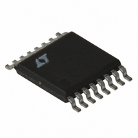
LT3431IFE#TR Linear Technology, LT3431IFE#TR Datasheet - Page 21

LT3431IFE#TR
Manufacturer Part Number
LT3431IFE#TR
Description
IC REG SW STDN 3A 500KHZ 16TSSOP
Manufacturer
Linear Technology
Type
Step-Down (Buck)r
Datasheet
1.LT3431EFEPBF.pdf
(28 pages)
Specifications of LT3431IFE#TR
Internal Switch(s)
Yes
Synchronous Rectifier
No
Number Of Outputs
1
Voltage - Output
1.2 ~ 48 V
Current - Output
3A
Frequency - Switching
500kHz
Voltage - Input
5.5 ~ 60 V
Operating Temperature
-40°C ~ 125°C
Mounting Type
Surface Mount
Package / Case
16-TSSOP Exposed Pad, 16-eTSSOP, 16-HTSSOP
Lead Free Status / RoHS Status
Contains lead / RoHS non-compliant
Power - Output
-
Available stocks
Company
Part Number
Manufacturer
Quantity
Price
APPLICATIO S I FOR ATIO
A detailed theoretical basis for estimating internal power
dissipation is given in the Thermal Calculations section.
This will allow a first pass check of whether an application’s
maximum input voltage requirement is suitable for the
LT3431. Be aware that these calculations are for DC input
voltages and that input voltage transients as high as 60V
are possible if the resulting increase in internal power
dissipation is of insufficient time duration to raise die
temperature significantly. For the FE package, this means
high voltage transients on the order of hundreds of milli-
seconds are possible. If LT3431 thermal calculations
show power dissipation is not suitable for the given
application, the LT3430 is a recommended alternative
since it is identical to the LT3431 but runs cooler at
200kHz.
Switch minimum on time is the other factor that may limit
the maximum operational input voltage for the LT3431 if
pulse-skipping behavior is not allowed. For the LT3431,
pulse-skipping may occur for V
(V
If the LT3430 is used, the ratio increases to 10. Pulse-
skipping is the regulator’s way of missing switch pulses to
maintain output voltage regulation. Although an increase
in output ripple voltage can occur during pulse-skipping,
a ceramic output capacitor can be used to keep ripple
voltage to a minimum (see output ripple voltage compari-
son for tantalum vs ceramic output capacitors, Figure 3).
FREQUENCY COMPENSATION
Before starting on the theoretical analysis of frequency
response, the following should be remembered—the worse
the board layout, the more difficult the circuit will be to
stabilize. This is true of almost all high frequency analog
circuits, read the Layout Considerations section first.
Common layout errors that appear as stability problems
are distant placement of input decoupling capacitor and/
or catch diode, and connecting the V
ground track carrying significant switch current. In addi-
F
= Schottky diode D1 forward voltage drop, Figure 5.)
U
U
IN
/(V
W
OUT
C
compensation to a
+ V
F
) ratios > 4.
U
tion, the theoretical analysis considers only first order
non-ideal component behavior. For these reasons, it is
important that a final stability check is made with produc-
tion layout and components.
The LT3431 uses current mode control. This alleviates
many of the phase shift problems associated with the
inductor. The basic regulator loop is shown in Figure 10.
The LT3431 can be considered as two g
amplifier and the power stage.
Figure 11 shows the overall loop response. At the V
the frequency compensation components used are:
R
capacitor used is a 100 F, 10V tantalum capacitor with
typical ESR of 100m .
The ESR of the tantalum output capacitor provides a
useful zero in the loop frequency response for maintain-
ing stability.
This ESR, however, contributes significantly to the ripple
voltage at the output (see Output Ripple Voltage in the
Applications Information section). It is possible to reduce
capacitor size and output ripple voltage by replacing the
LT3431
C
GND
CURRENT MODE
POWER STAGE
= 3.3k, C
g
m
= 2mho
V
R
C
C
C
200k
C
R
O
Figure 10. Model for Loop Response
C
2000 mho
= 0.022 F and C
g
C
AMPLIFIER
m
F
ERROR
=
–
+
1.22V
SW
FB
C
FB
F
= 220pF. The output
R
R1
R2
LOAD
m
blocks, the error
3431 F10
+
LT3431
TANTALUM
ESR
OUTPUT
C1
sn3431 3431fs
21
CERAMIC
C
pin,
ESL
C1


