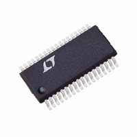
LTC1876EG#TRPBF Linear Technology, LTC1876EG#TRPBF Datasheet - Page 4

LTC1876EG#TRPBF
Manufacturer Part Number
LTC1876EG#TRPBF
Description
IC CTRLR/REG STEP UP/DOWN 36SSOP
Manufacturer
Linear Technology
Series
PolyPhase®r
Type
Step-Down (Buck), Step-Up (Boost)r
Datasheet
1.LTC1876EGPBF.pdf
(36 pages)
Specifications of LTC1876EG#TRPBF
Internal Switch(s)
No
Synchronous Rectifier
Yes
Number Of Outputs
3
Voltage - Output
Adj to 34V
Current - Output
1A
Frequency - Switching
140kHz ~ 340kHz
Voltage - Input
3.5 ~ 36 V
Operating Temperature
-40°C ~ 85°C
Mounting Type
Surface Mount
Package / Case
36-SSOP
Lead Free Status / RoHS Status
Lead free / RoHS Compliant
Power - Output
-
Available stocks
Company
Part Number
Manufacturer
Quantity
Price
LTC1876
ELECTRICAL CHARACTERISTICS
temperature range, otherwise specifications are at T
Note 1: Absolute Maximum Ratings are those values beyond which the life
of a device may be impaired.
Note 2: The LTC1876E is guaranteed to meet performance specifications
from 0 C to 70 C. Specifications over the – 40 C to 85 C operating
temperature range are assured by design, characterization and correlation
with statistical process controls.
Note 3: T
dissipation P
LTC1876EG: T
Note 4: The LTC1876 is tested in a feedback loop that servos V
specified voltage and measures the resultant V
4
SYMBOL
3.3V Linear Regulator
V
V
V
PGOOD Output
V
I
V
Aux Output
AUXV
AUXV
AUXI
AUXI
AUXV
AUXf
AUXDC
AUXI
AUXV
AUXI
AUXV
I
PGOOD
AUXSD
3.3OUT
3.3IL
3.3VL
PGL
PG
FB
Q
OSC
LIMIT
LEAKAGE
INMIN
FB
LINEREG
CESAT
AUXSD
MAX
J
is calculated from the ambient temperature T
D
J
according to the following formulas:
= T
PARAMETER
3.3V Regulator Output Voltage
3.3V Regulator Load Regulation
3.3V Regulator Line Regulation
PGOOD Voltage Low
PGOOD Leakage Current
PGOOD Trip Level, Either Controller
AUX Minimum Operating Voltage
AUX Regulated Feedback Voltage
AUX Feedback Pin Bias Current
AUX Input DC Supply Current
Normal Mode
Shutdown
AUX Line Regulation
AUX Oscillator Frequency
AUX Oscillator Maximum Duty Cycle
AUX Switch Current Limit
AUX Switch Saturation Voltage
AUX Switch Leakage Current
AUX Shutdown Input Voltage
AUXSD Pin Bias Current
AUX Shutdown Upper Trip Point
AUX Shutdown Lower Trip Point
A
V
V
+ (P
AUXSD
AUXSD
D
• 95 C/W)
= 3V
= 0V
OSENSE1, 2.
A
and power
CONDITIONS
No Load
I
6V < V
I
V
V
V
V
2.6V AUXV
(Note 9)
I
V
A
3.3
PGOOD
SW
PGOOD
OSENSE
AUXSD
AUXSD
SW
= 25 C. V
ITH1, 2
V
V
= 0mA to 10mA
= 900mA (Note 10)
= 5V
OSENSE
OSENSE
IN
= 2mA
The denotes the specifications which apply over the full operating
= 2.4V, Not Switching
= 0V
= 5V
with Respect to Set Output Voltage
< 30V
to a
Ramping Negative
Ramping Positive
IN
IN
= 15V, V
16V
Note 5: Dynamic supply current is higher due to the gate charge being
delivered at the switching frequency. See Applications Information.
Note 6: Rise and fall times are measured using 10% and 90% levels.
Delay times are measured using 50% levels.
Note 7: The minimum on-time condition is specified for an inductor peak-
to-peak ripple current 40% of I
Considerations in the Applications Information section).
Note 8: V
resistance.
Note 9: Current limit guaranteed by design and/or correlation to static test.
Note 10: 100% tested at wafer level.
RUN/SS1, 2
FREQSET
= 5V, AUXV
pin internally tied to 1.19V reference through a large
IN
MAX
= 3V unless otherwise noted.
(see Minimum On-Time
MIN
3.25
1.23
0.8
2.4
–6
84
6
1
–7.5
TYP
3.35
0.05
1.26
0.01
0.01
0.01
0.01
120
330
0.5
0.1
7.5
2.4
1.2
1.4
86
16
4
MAX
3.45
–9.5
1.28
0.05
360
550
0.2
0.3
9.5
2.6
1.6
0.5
0.1
32
2
1
2
1
1
UNITS
1876fa
MHz
%/V
mA
mV
nA
%
%
%
%
%
V
V
A
V
V
A
A
A
V
V
A
A


