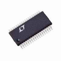
LTC1876EG#TRPBF Linear Technology, LTC1876EG#TRPBF Datasheet - Page 12

LTC1876EG#TRPBF
Manufacturer Part Number
LTC1876EG#TRPBF
Description
IC CTRLR/REG STEP UP/DOWN 36SSOP
Manufacturer
Linear Technology
Series
PolyPhase®r
Type
Step-Down (Buck), Step-Up (Boost)r
Datasheet
1.LTC1876EGPBF.pdf
(36 pages)
Specifications of LTC1876EG#TRPBF
Internal Switch(s)
No
Synchronous Rectifier
Yes
Number Of Outputs
3
Voltage - Output
Adj to 34V
Current - Output
1A
Frequency - Switching
140kHz ~ 340kHz
Voltage - Input
3.5 ~ 36 V
Operating Temperature
-40°C ~ 85°C
Mounting Type
Surface Mount
Package / Case
36-SSOP
Lead Free Status / RoHS Status
Lead free / RoHS Compliant
Power - Output
-
Available stocks
Company
Part Number
Manufacturer
Quantity
Price
LTC1876
OPERATIO
cycles, followed by a variable “sleep” interval depending
upon the load current. The resultant output voltage ripple
is held to a very small value by having the hysteretic
comparator after the error amplifier gain block.
Constant Frequency Operation
When the FCB pin is tied to INTV
is disabled and the forced minimum output current re-
quirement is removed. This provides constant frequency,
discontinuous (preventing reverse inductor current) cur-
rent operation over the widest possible output current
range. This constant frequency operation is not as efficient
as Burst Mode operation, but does provide a lower noise,
constant frequency operating mode down to approxi-
mately 1% of designed maximum output current.
Constant Current (PWM) Operation
Tying the FCB pin to ground will force continuous current
operation. This is the least efficient operating mode, but
may be desirable in certain applications. The output can
source or sink current in this mode. When sinking current
while in forced continuous operation, current will be
forced back into the main power supply potentially boost-
ing the input supply to dangerous voltage levels—
BEWARE!
Frequency Setting
The FREQSET pin provides frequency adjustment to the
controllers’ internal oscillator from approximately 140kHz
to 310kHz. This input is nominally biased through an
internal resistor to the 1.19V reference, setting the oscil-
lator frequency to approximately 220kHz. This pin can be
driven from an external AC or DC signal source to control
the instantaneous frequency of the oscillator. The auxillary
boost regulator operates at a constant 1.2MHz frequency.
INTV
Power for the top and bottom MOSFET drivers and most
other internal circuitry is derived from the INTV
When the EXTV
dropout linear regulator supplies INTV
is taken above 4.7V, the 5V regulator is turned off and an
internal switch is turned on connecting EXTV
12
CC
/EXTV
CC
Power
CC
U
pin is left open, an internal 5V low
(Refer to Functional Diagram)
CC
, Burst Mode operation
CC
power. If EXTV
CC
to INTV
CC
pin.
CC
CC
.
This allows the INTV
efficiency external source such as the output of the regu-
lator itself or a secondary winding, as described in Appli-
cations Information.
Standby Mode Pin
The STBYMD pin is a three-state input that controls
common circuitry within the IC as follows: When the
STBYMD pin is held at ground, both controller RUN/SS
pins are pulled to ground providing a single control pin to
shut down both controllers. When the pin is left open, the
internal RUN/SS currents are enabled to charge the
RUN/SS capacitor(s), allowing the turn-on of either con-
troller and activating necessary common internal biasing.
When the STBYMD pin is taken above 2V, both internal
linear regulators are turned on independent of the state of
the two switching regulator controllers, providing output
power to “wake-up” other circuitry. Decouple the pin with
a small capacitor (0.01 F) to ground if the pin is not
connected to a DC potential.
Output Overvoltage Protection
An overvoltage comparator, OV, guards against transient
overshoots (>7.5%) as well as other more serious condi-
tions that may overvoltage the output. In this case, the top
MOSFET is turned off and the bottom MOSFET is turned on
until the overvoltage condition is cleared.
Power Good (PGOOD) Pin
The PGOOD pin is connected to an open drain of an internal
MOSFET. The MOSFET turns on and pulls the pin low when
both the outputs are not within 7.5% of their nominal
output levels as determined by their resistive feedback
dividers. When both controller outputs meet the 7.5%
requirement, the MOSFET is turned off within 10 s and the
pin is allowed to be pulled up by an external resistor to a
source of up to 7V. The auxiliary regulator’s output is not
monitored.
Foldback Current, Short-Circuit Detection and Short-
Circuit Latchoff
The RUN/SS capacitors are used initially to limit the inrush
current of each step-down switching regulator. After the
CC
power to be derived from a high
1876fa


