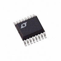
LTC1625IGN Linear Technology, LTC1625IGN Datasheet - Page 8

LTC1625IGN
Manufacturer Part Number
LTC1625IGN
Description
IC SW REG STEP-DOWN SYNC 16-SSOP
Manufacturer
Linear Technology
Type
Step-Down (Buck)r
Datasheet
1.LTC1625CSPBF.pdf
(24 pages)
Specifications of LTC1625IGN
Internal Switch(s)
No
Synchronous Rectifier
Yes
Number Of Outputs
1
Voltage - Output
1.19 ~ 36 V
Current - Output
50mA
Frequency - Switching
150kHz
Voltage - Input
3.7 ~ 36 V
Operating Temperature
-40°C ~ 85°C
Mounting Type
Surface Mount
Package / Case
16-SSOP
Lead Free Status / RoHS Status
Contains lead / RoHS non-compliant
Power - Output
-
Available stocks
Company
Part Number
Manufacturer
Quantity
Price
Part Number:
LTC1625IGN
Manufacturer:
LINEAR/凌特
Quantity:
20 000
Part Number:
LTC1625IGN#PBF
Manufacturer:
LINEAR/凌特
Quantity:
20 000
Part Number:
LTC1625IGN#TRPBF
Manufacturer:
LINEAR/凌特
Quantity:
20 000
LTC1625
OPERATIO
Main Control Loop
The LTC1625 is a constant frequency, current mode
controller for DC/DC step-down converters. In normal
operation, the top MOSFET is turned on when the RS latch
is set by the on-chip oscillator and is turned off when the
current comparator I
MOSFET is turned off, the bottom MOSFET is turned on
until either the inductor current reverses, as determined
by the current reversal comparator I
begins. Inductor current is measured by sensing the V
potential across the conducting MOSFET. The output of
the appropriate sense amplifier (TA or BA) is selected by
the switch logic and applied to the current comparator.
The voltage on the I
corresponding to peak inductor current. The error ampli-
fier EA adjusts this voltage by comparing the feedback
signal V
reference. The V
voltage is taken directly from the V
from an on-chip resistive divider. When the load current
increases, it causes a drop in the feedback voltage relative
to the reference. The I
average inductor current again matches the load current.
The internal oscillator can be synchronized to an external
clock applied to the SYNC pin and can lock to a frequency
between 100% and 150% of its nominal 150kHz rate.
When the SYNC pin is left open, it is pulled low internally
and the oscillator runs at its normal rate. If this pin is taken
above 1.2V, the oscillator will run at its maximum 225kHz
rate.
Pulling the RUN/SS pin low forces the controller into its
shutdown state and turns off both MOSFETs. Releasing
the RUN/SS pin allows an internal 3 A current source to
charge up an external soft start capacitor C
voltage reaches 1.4V, the controller begins switching, but
with the I
C
operation is restored.
The top MOSFET driver is powered from a floating boot-
strap capacitor C
from INTV
turned off. As V
8
SS
continues to charge, the clamp is raised until full range
FB
TH
CC
from the output voltage with the internal 1.19V
voltage clamped at approximately 0.8V. As
through a diode D
IN
PROG
B
U
decreases towards V
. This capacitor is normally recharged
TH
1
pin sets the comparator threshold
pin selects whether the feedback
resets the latch. While the top
TH
voltage then rises until the
B
when the top MOSFET is
OSENSE
2
, or the next cycle
OUT
pin or is derived
, the converter
SS
. When this
DS
will attempt to turn on the top MOSFET continuously
(‘’dropout’’). A dropout counter detects this condition and
forces the top MOSFET to turn off for about 500ns every
tenth cycle to recharge the bootstrap capacitor.
An overvoltage comparator OV guards against transient
overshoots and other conditions that may overvoltage the
output. In this case, the top MOSFET is turned off and the
bottom MOSFET is turned on until the overvoltage condi-
tion is cleared.
Foldback current limiting for an output shorted to ground
is provided by a transconductance amplifer CL. As V
drops below 0.6V, the buffered I
comparator is gradually pulled down to a 0.95V clamp.
This reduces peak inductor current to about one fifth of its
maximum value.
Low Current Operation
The LTC1625 is capable of Burst Mode operation at low
load currents. If the error amplifier drives the I
below 0.95V, the buffered I
parator will remain clamped at 0.95V. The inductor current
peak is then held at approximately 30mV/R
I
will turn off both MOSFETs. The load current will be
supplied solely by the output capacitor until I
above the 50mV hysteresis of the comparator and switch-
ing is resumed. Burst Mode operation is disabled by
comparator F when the FCB pin is brought below 1.19V.
This forces continuous operation and can assist second-
ary winding regulation.
INTV
Power for the top and bottom MOSFET drivers and most
of the internal circuitry of the LTC1625 is derived from the
INTV
5.2V low dropout regulator supplies the INTV
from V
regulator is turned off and an internal switch connects
EXTV
such as the primary or a secondary output of the converter
itself, to provide the INTV
TH
then drops below 0.5V, the Burst Mode comparator B
CC
CC
CC
/EXTV
IN
pin. When the EXTV
to INTV
. If EXTV
CC
CC
Power
. This allows a high efficiency source,
CC
is raised above 4.7V, the internal
CC
CC
TH
power.
pin is left open, an internal
input to the current com-
TH
input to the current
DS(ON)(TOP)
TH
CC
TH
voltage
power
rises
. If
FB


